Ver 1.3
PRELIMINARY
EAGLE
3.3.5 Texture Memory Control Register (TMEMCON)
Bank 7 belongs to the texture memory region. It can be connected to SDRAM
* Notice : Supports SDRAM in Full Page Burst mode only.
DMA transfer should be aligned to the transfer block size to avoid page-miss,. For example, a word transfer with transfer
size of 16 requires the set-up of DMA Source/Destination Address at the border of 16 word.
Bank 7 allows the usage of two SDRAM by extending the addresses linearly. The chip select signal for each of the
SDRAM is known as TSD_CSx and TSD_CSx2, respectively.
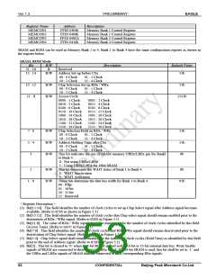
Register Name
Address
Description
TMEMCON
FFE0 0430h
Texture Memory Control Register (SDRAM)
Bit
31 : 17
16
R/W
R
R/W
Description
Default Value
Reserved
-
0b
Texture Memory Access Enable
0 : Access Inactivation
1 : Access Activation
Reserved
15 : 8
7 : 6
R
R/W
-
Row Address Line Number
11b
00 : 11 bit
10 : 13 bit
01 : 12 bit
11 : Reserved
5 : 4
R/W
R/W
Column Address Line Number
11b
0b
00 : 8 bit
01 : 9 bit
10 : 10 bit
11 : Reserved
3
Timing Constraint Select ( 0 : greater than 100MHz, 1 : less than 100
MHz)
0 : tRCD = 3 Clock, tRP = 3 Clock, tRAS = 7 Clock, tRC = 10 Clock
1 : tRCD = 2 Clock, tRP = 2 Clock, tRAS = 5 Clock, tRC = 7 Clock
CAS Latency
2
R/W
0b
0 : 2 Clock
1 : 3 Clock
1
0
R
R
Reserved
-
0b
This bit determines data bus width for bank 7
16 bit only
< Register Description >
(1) Bit[16] : This field determines whether Texture Memory is enabled or disabled.
(2) Bit[7:6] : This field selects the number of Row Address in SDRAM.
(3) Bit[5:4] : This field selects the number of Column Address in SDRAM .
Bit[3] : This field determines the timing constraint for SDRAM operation. The threshold value is set at
100MHz. When more than 100 MHz is detected, adjust the timing by setting this bit to ‘0’..
(4) Bit[2] : In SDRAM operation, CAS Latency Cycle is selected.
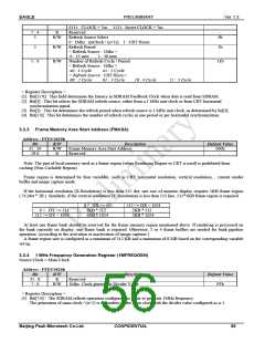
3.3.6 Texture SDRAM Clock Delay & Refresh Control (TMEMCLKCON)
Address : FFE0 0434h
Bit
31 : 12
11 : 8
R/W
R
R/W
Description
Default Value
Reserved
Texture SDRAM Clock Generation (Clock Delay)
0000 : CLOCK 1000 : Invert CLOCK
-
0h
0001 : CLOCK + 1ns 1001 : Invert CLOCK + 1ns
0010 : CLOCK + 2ns 1010 : Invert CLOCK + 2ns
0011 : CLOCK + 3ns 1011 : Invert CLOCK + 3ns
0100 : CLOCK + 4ns 1100 : Invert CLOCK + 4ns
0101 : CLOCK + 5ns 1101 : Invert CLOCK + 5ns
0110 : CLOCK + 6ns 1110 : Invert CLOCK + 6ns
0111 : CLOCK + 7ns 1111 : Invert CLOCK + 7ns
Reserved
7 : 2
1
R
R/W
-
1b
Refresh Period
< Refresh Source : 1MHz >
0 : 15 usec
1 : 30 usec
57
CONFIDENTIAL
Beijing Peak Microtech Co.Ltd.

 ETC [ ETC ]