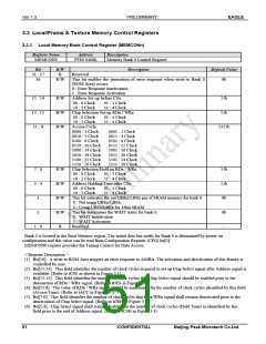
Ver 1.3
PRELIMINARY
EAGLE
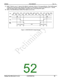
(4) Bit[11:8] : The value of RDx / WRx signal should be maintained for the number of clock cycles identified by this field
(Access Time). (Refer to tACC in Figure 3.1)
(5) Bit[7:6] : This field identifies the number of clock cycles that RDx/WRx signal should remain deactivated prior to the
deactivation of Chip Select signal. (Refer to tOEH in Figure 3.1)
(6) Bit[5:4] : Chip Select signal shall remain disabled for the number of clock cycles (Hold Time) as identified by this field
prior to the end of Address signal. (Refer to tCSH in Figure 3.1)
(7) Bit[3] : This bit is cleared to ‘0’ when an 8-bit SRAM is used with a 16-bit or 32-bit external data bus. Write Enable
signals of SRAM are connected to their respective BEx signal. If a 16-bit SRAM is used, this bit shall be set to ‘1’ and
the UBEx and LBEx signals of SRAM shall be connected to their corresponding BEx signals.
(8) Bit[2] : To determine whether Wait signal is in-use or not.
(9) Bit[1:0] : These bits identify the data bus width of ROM/SRAM/IO for Bank 5 and Bank 6.
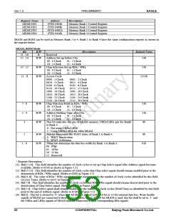
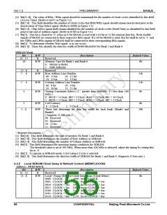
SDRAM Mode
Bit
31 : 17
16
R/W
R
R/W
Description
Default Value
Reserved
-
0b
Memory Type for Bank 5 and Bank 6
0 : SRAM or ROM
1 : SDR SDRAM
15 : 8
7 : 6
R
R/W
Reserved
Row Address Line Number
-
11b
00 : 11 bit
10 : 13 bit
01 : 12 bit
11 : 14 bit
5 : 4
R/W
R/W
Column Address Line Number
11b
0b
00 : 8 bit
01 : 9 bit
10 : 10 bit
11 : 11 bit
3
Timing Constraint Select ( 0 : greater than 100MHz, 1 : less than 100
MHz )
0 : tRCD = 3 Clock, tRP = 3 Clock, tRAS = 7 Clock, tRC = 10 Clock
1 : tRCD = 2 Clock, tRP = 2 Clock, tRAS = 5 Clock, tRC = 7 Clock
CAS Latency
2
R/W
R/W
0b
0 : 2 Clock
1 : 3 Clock
1 : 0
These bits determine the data bus width for each bank. (Bank5 and
10b
Bank6)
( Supports 32 bits only )
00 : Reserved
01 : Reserved
10 : 32 bit
11 : Reserved
< Register Description >
(1) Bit[16] : This field determines the type of memory for Bank 5 and Bank 6.
(2) Bit[7:6] : This field determines the number of Row Address in SDRAM.
(3) Bit[5:4] : This field determines the number of Column Address in SDRAM.
(4) Bit[3] : This field determines the operating timing conditions for SDRAM.
The threshold value is set at 100 MHz. When more than 100 MHz is detected, adjust the timing by setting this
bit to ‘0’.
(5) Bit[2] : To operate in SDRAM mode, CAS Latency Cycle is selected,
(6) Bit[1:0] : This field determines the data bus width of SDRAM for Bank 5 and Bank 6. (Supports 32 bits only ).
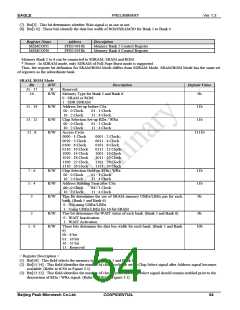
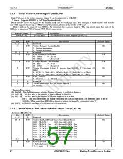
3.3.2 Local SDRAM Clock Delay & Refresh Control (MEMCLKCON)
Address : FFE0 041Ch
Bit
31 : 12
11 : 8
R/W
R
R/W
Description
Default Value
Reserved
Local / Frame SDRAM Clock Generation (Clock Delay)
0000 : CLOCK 1000 : Invert CLOCK
-
0h
0001 : CLOCK + 1ns 1001 : Invert CLOCK + 1ns
0010 : CLOCK + 2ns 1010 : Invert CLOCK + 2ns
0011 : CLOCK + 3ns 1011 : Invert CLOCK + 3ns
0100 : CLOCK + 4ns 1100 : Invert CLOCK + 4ns
0101 : CLOCK + 5ns 1101 : Invert CLOCK + 5ns
0110 : CLOCK + 6ns 1110 : Invert CLOCK + 6ns
55
CONFIDENTIAL
Beijing Peak Microtech Co.Ltd.

 ETC [ ETC ]