EAGLE
PRELIMINARY
Ver 1.3
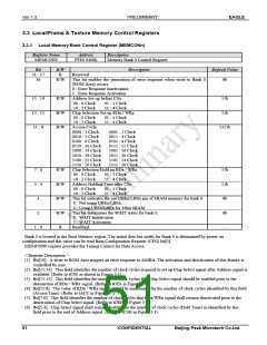
(7) Bit[2] : This bit determines whether Wait signal is in-use or not.
(8) Bit[1:0] : These bits identify the data bus width of ROM/SRAM/IO for Bank 1 to Bank 4.
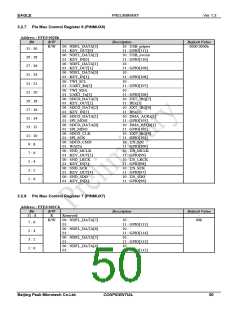
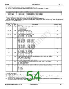
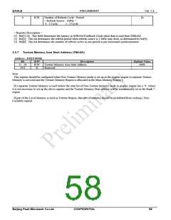
Register Name
MEMCON5
MEMCON6
Address
FFE0 0414h
FFE0 0418h
Description
Memory Bank 5 Control Register
Memory Bank 6 Control Register
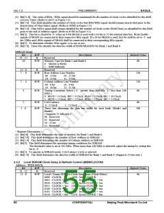
Memory Bank 5 to 6 can be connected to SDRAM, SRAM and ROM.
* Notice : In SDRAM mode, only SDRAM of Full Page Burst mode is supported.
Thus, the register bit definition for SRAM/ROM Mode differs from SDRAM Mode. SRAM/ROM Mode has the same set
of registers as the subordinate bank.
SRAM, ROM Mode
Bit
31 : 17
16
R/W
R
R/W
Description
Default Value
Reserved
-
0b
Memory Type for Bank 5 and Bank 6
0 : SRAM or ROM
1 : SDR SDRAM
15 : 14
13 : 12
11 : 8
R/W
R/W
R/W
Address Set-up before CSx
11b
11b
00 : 0 Clock
10 : 2 Clock
01 : 1 Clock
11 : 4 Clock
Chip Selection Set-up RDx / WRx
00 : 0 Clock
10 : 2 Clock
01 : 1 Clock
11 : 4 Clock
Access Cycle
0000 : 1 Clock
0010 : 3 Clock
0100 : 6 Clock
0110 : 10 Clock
1000 : 14 Clock
1010 : 18 Clock
1100 : 22 Clock
1110 : 26 Clock
1111b
0001 : 2 Clock
0011 : 4 Clock
0101 : 8 Clock
0111 : 12 Clock
1001 : 16 Clock
1011 : 20 Clock
1101 : 24 Clock
1111 : 30 Clock
7 : 6
5 : 4
3
R/W
R/W
R/W
Chip Selection Hold on RDx / WRx
11b
11b
0b
00 : 0 Clock
10 : 2 Clock
01 : 1 Clock
11 : 4 Clock
Address Holding Time after CSx
00 : 0 Clock
10 : 2 Clock
01 : 1 Clock
11 : 4 Clock
This bit determines the use of SRAM memory UBEx/LBEx pin for each
bank. (Bank 5 and Bank 6)
0 : Not using UBEx/LBEx
1 : Using UBEx/LBEx for 16-bit SRAM
2
R/W
R/W
This bit determines the WAIT status of each bank. (Bank 5 and Bank 6)
0 : WAIT Inactivation
1 : WAIT Activation
These bits determine the data bus width for each bank. (Bank 5 and Bank
0b
1 : 0
10b
6)
00 : 8 bit
01 : 16 bit
10 : 32 bit
11 : Reserved
< Register Description >
(1) Bit[16] : This field selects the memory type of Bank 5 and Bank 6
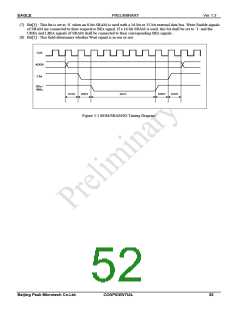
(2) Bit[15:14] : This field identifies the number of clock cycles to set up Chip Select signal after Address signal becomes
available. (Refer to tCSS in Figure 3.1)
(3) Bit[13:12] : This field identifies the number of clock cycles that Chip select signal should remain enabled prior to the
deassertion of RDx / WRx signal. (Refer to tOES in Figure 3.1)
Beijing Peak Microtech Co.Ltd.
CONFIDENTIAL
54

 ETC [ ETC ]