EAGLE
PRELIMINARY
Ver 1.3
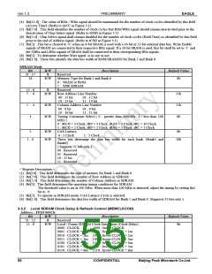
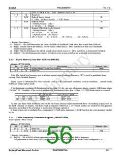
0111 : CLOCK + 7ns 1111 : Invert CLOCK + 7ns
Reserved
7 : 4
R
-
3
R/W
Refresh Source Select
0b
0 : 1Mhz (mClock / (n+1)) 1 : CRT Hsync
2
R/W
R/W
Refresh Period
< Refresh Source : 1Mhz >
0 : 15 usec
Number of Refresh Cycle / Period
< Refresh Source : 1Mhz >
1b
1 : 30 usec
1 : 0
11b
x0 : 1 Cycle
< Refresh Source : CRT Hsync>
00 : 2 Cycle 01 : 3 Cycle
x1 : 2 Cycle
10 : 4 Cycle
11 : 5 Cycle
< Register Description >
(1) Bit[11:8] : This field determines the latency in SDRAM Feedback Clock when data is read from SDRAM.
(2) Bit[3] : This bit selects the SDRAM refresh source, either from a 1 MHz unit clock or from CRT horizontal
synchronization signal.
(3) Bit[2] : This bit determines the refresh period when refresh source is 1 MHz unit clock, as determined by bit[3].
(4) Bit[1:0] : This bit determines the number of refresh cycles in one period or per horizontal synchronization.
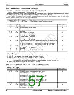
3.3.3 Frame Memory Area Start Address (FMASA)
Address : FFE0 0420h
Bit
31 : 20
19:0
R/W
R/W
R
Description
Frame Memory Area Start Address
Reserved
Default Value
000h
-
Note: The part of local memory used as a frame region (when Rendering Engine or CRT is used) is prohibited from
caching (Non-Cachable Region).
Frame region is determined by four variables, such as CRT horizontal resolution, vertical resolution, , current render
buffer and image capture mode.
If the horizontal resolution (X-Resolution) is less than 512 dot, one row of monitor display requires 1KB frame region
( 512dot * 2B ). Similarly, if the vertical resolution (Y-Resolution) is less than 512 line, 512*1KB frame region is required.
0 < DX <= 511
1KB * 512
512 <= DX < 1024
2KB * 512
0 < DY <= 511
512 <= DY < 1024
1KB * 1024
2KB * 1024
At least one frame bank should be reserved for the frame memory region mentioned above. If rendering is processed on
the bank currently on display, one frame bank is required. Otherwise, 2 or 4 frame buffers are needed for bank pipeline
operation. (according to the activation or inactivation of image capturer )
A frame region size is configured as a minimum of 512 KB and a maximum of 8 MB based on the corresponding variable
set-up,
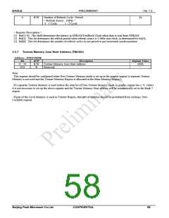
3.3.4 1 MHz Frequency Generation Register (1MFREQGEN)
Source Clock = Main Clock
Address : FFE0 0424h
Bit
31 : 8
7 : 0
R/W
R
R/W
Description
Reserved
1Mhz Clock generation Divider Value
Default Value
-
FFh
< Register Description >
(1) Bit[7:0] : The SDRAM refresh operation configures the value to generate 1MHz frequency.
The generation of main clock / (n+1) is dependent on the main clock with the divider value configured as n-1.
Beijing Peak Microtech Co.Ltd.
CONFIDENTIAL
56

 ETC [ ETC ]