Proprietary TranSwitch Corporation Information for use Solely by its Customers
L3M
TXC-03452B
DATA SHEET
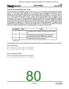
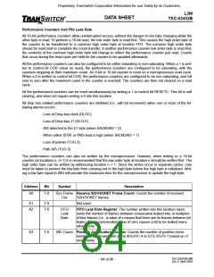
The “O”-bits consists of two overhead communication bits per subframe, for nine subframes, in the DS3 format,
or for 3 subframes in the E3 format. The selection of the two bits per subframe, either from the “O”-bit interface
or from RAM, operates in the same way as the Path Overhead bytes, but “O”-bits from the transmit “O”-bit port
are not written into RAM. When sourced from the RAM, the same “O”-bit pair will be sent throughout the entire
SONET frame (i.e., the “O”-bit value from RAM is accessed only once per frame).
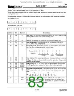
Address
Bit
Symbol
Description
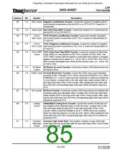
00
to
3F
7-0
J1
Path Trace: The bytes written into this location provide a repetitive 64 byte
fixed length message for transmission. The bytes written into these posi-
tions are either from the microprocessor or from the external POH I/O.
40
7-0
B3
Error
Mask
B3 Error Mask: When control bit TESTB3 is a 0, the bit columns written
with a one represent the columns in the B3 byte in which errors are gener-
ated. The B3 errors are sent until this position is rewritten with a 00H.
When control bit TESTB3 is a 1, the value written into this location is the
transmitted B3 byte.
41
42
7-0
7-0
C2
G1
Path Signal Label (microprocessor): The bits written into this position
indicate the construction of the AU-3, TUG-3, or SPE.
Transmit Byte G1: This byte is used for sending the microprocessor-con-
trolled states for FEBE, RDI, and the unassigned bits, according to states
given in the tables below:
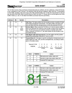
Transmit G1 Bit
RAM Bit
1
7
2
6
3
5
4
4
5
3
6
2
7
1
8
0
TFEBE
TRDI
Unassigned
TFEBE
EXG1
FEBEEN
Action
0
0
1
0
1
Microprocessor-written value sent
Internal or mate (ring mode) value sent
External POH value sent
X
TRDI
EXG1
RAMRDI
Action
0
0
1
0
1
Internal or mate (ring mode) value sent
Microprocessor-written value sent
External POH value sent
X
Unassigned Bits
EXG1
Action
0
1
Microprocessor-written value sent
External POH value sent
TXC-03452B-MB
Ed. 6, April 2001
- 81 of 96 -

 ETC [ ETC ]