Proprietary TranSwitch Corporation Information for use Solely by its Customers
L3M
TXC-03452B
DATA SHEET
Address
Bit
Symbol
Description
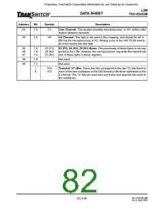
43
7-0
F2
User Channel: This location provides microprocessor- or I/O- written infor-
mation between elements.
44
7-0
H4
H4 Channel: This byte is not used in this mapping, and should be set to
00H by the microprocessor or I/O. Writing a one to the H4CTR bit inserts
an 8-bit counter into this byte.
45
46
47
7-0
7-0
7-0
Z3 (F3)
Z4 (K3)
Z5 (N1)
Z3 (F3), Z4 (K3), Z5 (N1) Bytes: The processing of these bytes is not sup-
ported in the L3M. However, the microprocessor may write the transmit val-
ues of these bytes in these registers.
48
49
7-0
7-2
Not used.
Not used.
1
0
TO2
TO1
Transmit “O”-Bits: These two bits correspond to the two “O”-bits found in
each of the nine subframes in the DS3 format or the three subframes in the
E3 format. The “O”-bits are read once per frame and inserted into each of
the subframes.
TXC-03452B-MB
Ed. 6, April 2001
- 82 of 96 -

 ETC [ ETC ]