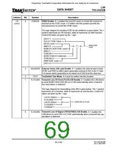
Proprietary TranSwitch Corporation Information for use Solely by its Customers
L3M
TXC-03452B
DATA SHEET
Address
Bit
Symbol
Description
C7
7
TESTB3
Test B3 Byte: A 1 transmits a B3 value written by the microprocessor in
location 40H. A 0 enables the test byte to become a test mask. When con-
figured as a test mask, a 1 in one or more bit positions causes those bits in
the transmitted B3 byte to be inverted.
6
FIXPTR
TUG-3 Fixed Pointer Generation: A 1 forces a fixed pointer of 0 to be
generated in the transmitted TUG-3 regardless of any pointer movements
(J1 in DC1J1) that may occur on the Drop side when the Drop timing mode
is selected, or if a pointer movement (J1 in AC1J1) takes place when Add
bus timing is selected. When this bit is written with a 0, a pointer movement
on the Add or Drop bus is compensated with an outgoing TUG-3 pointer
movement in the opposite direction.
5
4
TEST
DIV4
Test Bit Position: This bit must be set to 1.
Phase Detector Gain: This control bit governs the gain of the phase
detector, and it should be set as indicated in the Operation section entitled
“PLL Filter Connection to VCXO”.
3
2
1
INVCTRL Invert Control: Inverts the CTRL output lead (lead 3 or D3). When set to
0, the external loop filter must be non-inverting, which requires the use of
an inverter in the loop (U1 in Figure 32). When set to 1, an external invert-
ing loop filter is necessary, and U1 is not required.
TXRST
Transmit Reset: A 1 written into this position resets the transmit section
(Line to SDH/SONET) of the L3M device. This includes the transmit FIFOs
and internal counters. The L3M device’s transmitter will remain reset until
the microprocessor writes a 0 into this location.
RXRST
Receive Reset: A 1 written into this position resets the receive section
(SDH/SONET to Line) of the L3M device. This includes the receive FIFOs
and internal counters. The L3M device’s receiver will remain reset until the
microprocessor writes a 0 into this location.
0
RESETC Reset Performance Counters: A 1 written into this position resets all per-
formance counters to 0. This bit is self clearing, and does not require the
microprocessor to write a 0 into this location.
C8
C9
7-0
C2 Compare Path Signal Label Compare: The bits in this location are written by the
microprocessor, and are compared against the C2 byte received (register
91H) for a signal label mismatch condition.
7-2
1
TEST
RDI5
Test Bit Positions: Zeros must be written into these bits.
RDI 5 Consecutive Enable: A 1 enables the detection/recovery of RDI (bit
5 in the G1 byte) to 5 consecutive matches/mismatches. A 0 enables the
detection/recovery of RDI to 10 consecutive matches/mismatches.
0
FEBEBLK FEBE Counter Block Count Enable: A 1 configures the FEBE counter
(register locations AA and AB) to count one or more FEBE errors per
received G1 byte as one error (block). A 0 configures the FEBE counter to
count the number of errors detected (1 to 8).
TXC-03452B-MB
Ed. 6, April 2001
- 73 of 96 -

 ETC [ ETC ]