Proprietary TranSwitch Corporation Information for use Solely by its Customers
L3M
TXC-03452B
DATA SHEET
Address
Bit
Symbol
Description
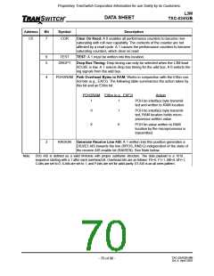
C5
7
COR
Clear On Read: A 0 enables all performance counters to become non-
saturating with roll over capability. The contents of the counter are not
affected by a read cycle. A 1 causes the performance counters to become
saturating counters, which clear on read.
6
5
TEST
TEST: A 1 must be written into this location.
DROPT
Drop Bus Timing: Drop timing can only be selected when the L3M lead
XCLKE is low. A 1 selects drop bus timing for the add bus. A 0 selects tim-
ing signals from the add bus.
4
POH2RAM Path Overhead Bytes to RAM: Works in conjunction with the EXbn con-
trol bits (e.g., EXF2). The following table summarizes the action taken by
this bit and an EXbn bit:
POH2RAM EXbn (e.g., EXF2)
Action
1
1
POH bn interface byte transmit-
ted and written to RAM location.
0
1
POH bn interface byte transmit-
ted, RAM location holds micro-
processor-written value.
X
0
POH bn value written to RAM
location by the microprocessor is
transmitted.
3
RAISGN
Generate Receive Line AIS: A 1 written into this position generates a
DS3/E3 AIS towards the line (RPOS, RNEG) independent of the state of
the receive AIS enable bit (RAISEN). See Note below.
Note:
DS3 AIS is defined as a valid M-frame with proper subframe structure. The data payload is a 1010...
sequence starting with a 1 after each overhead bit. Overhead bits are as follows: F0=0, F1=1, M0=0, M1=1;
C-bits are set to 0; X-bits are set to 1; and P-bits are set for valid parity. E3 AIS is an all ones pattern.
TXC-03452B-MB
Ed. 6, April 2001
- 70 of 96 -

 ETC [ ETC ]