Proprietary TranSwitch Corporation Information for use Solely by its Customers
L3M
TXC-03452B
DATA SHEET
Address
Bit
Symbol
Description
C4
(cont.)
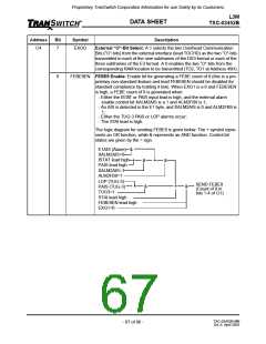
4
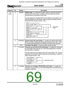
FEBEEN FEBE Enable: A 1 enables the local B3 count or remote B3 count to be
inserted as the FEBE count. A 0 written into this position permits the
microprocessor to control the FEBE count.
The logic diagram for sending FEBE for all conditions is given below. The +
symbol represents an OR function, while & represents an AND function.
Control bit states are given by the = sign.
EXG1=1
Port G1 FEBE Value
RX B3 count
RING=0
&
&
SEND FEBE
Count
+
+
+
&
&
REMOTE ALM FEBE count
RING=1
&
FEBEEN=1
SEND FEBE9=0 (internal)
FEBEEN=0
RAM FEBE count
EXG1=0
&
3
XALM2AIS External Alarm AIS Lead Enable: A 1 enables the external alarm leads
(ISTAT and PAIS) to affect alarm generation instead of AIS in the E1 byte.
A 0 causes alarm generation to be based on E1AIS from the drop bus.
2
1
TEST
TranSwitch Test Mode: A 0 must be written into this location.
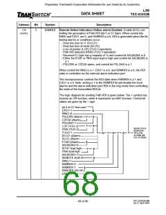
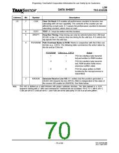
TLOC2AIS Transmit Loss Of Clock (TLCK) AIS Enable: A 1 enables the L3M device
to send SONET/SDH DS3 AIS or E3 AIS automatically when a transmit
line clock failure is detected.
The logic diagram for transmitting a line AIS is given below. The + symbol
represents an or function, while & represents an and function. Control bit
states are given by the = sign.
L3LOC (Alarm)
TLOC2AIS=1
L3LOS (Alarm)
TLOS2AIS=1
TLAISGN=1
&
&
+
SEND DS3 or E3 AIS
0
TLOS2AIS Transmit Loss Of Signal (TPOS/TNEG) AIS Enable: A 1 enables the
L3M device to send DS3 or E3 AIS automatically when a transmit line sig-
nal failure is detected.
TXC-03452B-MB
Ed. 6, April 2001
- 69 of 96 -

 ETC [ ETC ]