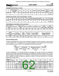
Proprietary TranSwitch Corporation Information for use Solely by its Customers
L3M
TXC-03452B
DATA SHEET
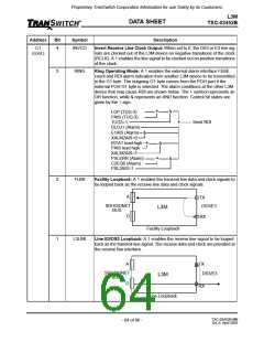
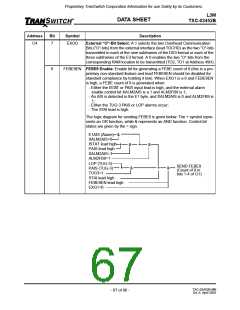
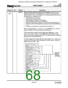
Address
Bit
Symbol
Description
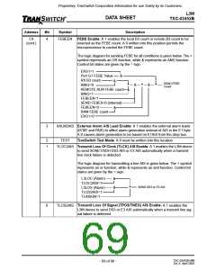
C2
(cont.)
2
INTZ
Interrupt High Impedance Enable: A 0 enables the interrupt INT/IRQ
(lead 129 or B8) to be either high (Intel mode) with the off state low, or to
be low (Motorola mode), with the off state high. A 1 enables the off state to
be high impedance.
1
ADDZ
Add Bus High Impedance Enable: A 1 sets Add bus data (ADATA(7-0))
and Add Parity (APAR) leads to a high impedance state, and ADD high. If
the external timing mode is selected, the clock (ACLK), SPE (ASPE), and
C1J1 (AC1J1) signals are also forced to a high impedance state.
0
7
6
5
4
3
2
L3Z
Receive Output High Impedance Enable: A 1 forces the receive inter-
face clock (RCLK) and data signals (RPOS and RNEG), and NRZ outputs
(RNRZC and RNRZD) to a high impedance state.
C3
EXZ5
EXZ4
EXZ3
EXH4
EXF2
EXG1
Transmit External Interface Z5 byte: A 1 enables the Z5 byte from the
POH I/O to be transmitted. A 0 enables the corresponding RAM location to
be transmitted.
Transmit External Interface Z4 byte: A 1 enables the Z4 byte from the
POH I/O to be transmitted. A 0 enables the corresponding RAM location to
be transmitted.
Transmit External Interface Z3 byte: A 1 enables the Z3 byte from the
POH I/O to be transmitted. A 0 enables the corresponding RAM location to
be transmitted.
Transmit External Interface H4 byte: A 1 enables the H4 byte from the
POH I/O to be transmitted. A 0 enables the corresponding RAM location to
be transmitted.
Transmit External Interface F2 byte: A 1 enables the F2 byte from the
POH I/O to be transmitted. A 0 enables the corresponding RAM location to
be transmitted.
Transmit External Interface G1 Byte: A 1 enables bits 1 through 8 in the
G1 byte from the POH I/O to be transmitted. A 0 enables the correspond-
ing RAM location or internal logic/alarms to control the transmitted state of
FEBE, RDI, and the unassigned bits.
1
0
EXC2
EXJ1
Transmit External Interface C2 Byte: A 1 enables the C2 byte from the
POH I/O to be transmitted. A 0 enables the corresponding RAM location to
be transmitted.
Transmit External Interface J1 Bytes: A 1 enables the J1 bytes from the
POH I/O to be transmitted. A 0 enables the corresponding RAM segment
(64 locations) to be transmitted.
TXC-03452B-MB
Ed. 6, April 2001
- 66 of 96 -

 ETC [ ETC ]