Proprietary TranSwitch Corporation Information for use Solely by its Customers
L3M
TXC-03452B
DATA SHEET
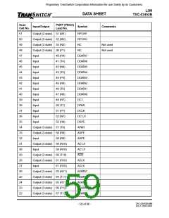
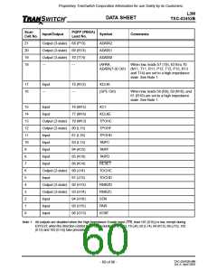
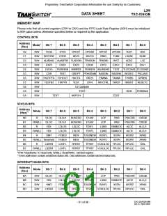
MEMORY MAP DESCRIPTIONS
CONTROL BITS
On power-up, the control bits will not be automatically initialized to a fixed default pattern. The microprocessor
must write the control bits to the required system status. The control bits are not affected by either hardware or
software resets.
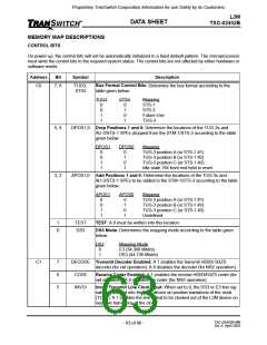
Address
Bit
Symbol
Description
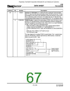
C0
7, 6
TUG3,
STS3
Bus Format Control Bits: Determine the bus format according to the
table given below:
TUG3
STS3
Mapping
STS-1
STS-3
Future Use
TUG-3
0
0
1
1
0
1
0
1
5, 4
DPOS1,0 Drop Positions 1 and 0: Determine the locations of the TUG-3s and
AU-3/STS-1 SPEs dropped from the STM-1/STS-3 according to the table
given below:
DPOS1
DPOS0
Mapping
0
0
1
1
0
1
0
1
TUG-3 position A (or STS-1 #1)
TUG-3 position B (or STS-1 #2)
TUG-3 position C (or STS-1 #3)
Idle state. RX front end held in reset.
3, 2
APOS1,0 Add Positions 1 and 0: Determine the locations of the TUG-3s and
AU-3/STS-1 SPEs to be added to the STM-1/STS-3 according to the table
given below:
APOS1
APOS0
Mapping
0
0
1
1
0
1
0
1
TUG-3 position A (or STS-1 #1)
TUG-3 position B (or STS-1 #2)
TUG-3 position C (or STS-1 #3)
Undefined
1
0
TEST
DS3
TEST: A 0 must be written into this location.
DS3 Mode: Determines the mapping mode according to the table given
below:
DS3
0
1
Mapping Mode
E3 (34.368 Mbit/s)
DS3 (44.736 Mbit/s)
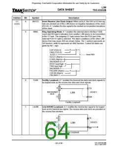
C1
7
6
5
DECODE Transmit Decoder Enabled: A 1 enables the transmit HDB3/ B3ZS
decoder (for rail operation). A 0 disables the decoder (for NRZ operation).
CODE
INVCI
Receive Coder Enabled: A 1 enables the receive HDB3/B3ZS coder (for
rail operation). A 0 disables the coder (for NRZ operation).
Invert Transmit Line Clock Input: When set to 0, the DS3 or E3 line sig-
nals are clocked into the L3M device on positive transitions of the clock
(TCLK). A 1 enables the line signal to be clocked out of the L3M device on
negative transitions of the clock.
TXC-03452B-MB
Ed. 6, April 2001
- 63 of 96 -

 ETC [ ETC ]