Proprietary TranSwitch Corporation Information for use Solely by its Customers
L3M
TXC-03452B
DATA SHEET
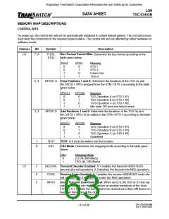
Address
Bit
Symbol
Description
C1
(cont.)
4
INVCO
Invert Receive Line Clock Output: When set to 0, the DS3 or E3 line sig-
nals are clocked out of the L3M device on negative transitions of the clock
(RCLK). A 1 enables the line signal to be clocked out on positive transitions
of the clock.
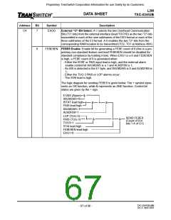
3
RING
Ring Operating Mode: A 1 enables the external alarm interface FEBE
count and RDI alarm indication from another L3M device to be transmitted
in the G1 byte. The outgoing G1 byte comes from the POH port if the
external POH G1 byte is selected. The alarm conditions at the other L3M
device that may cause RDI are shown below. The + symbol represents an
OR function, while & represents an AND function. Control bit states are
given by the = sign.
+
&
LOP (TUG-3)
PAIS (TUG-3)
TUG3=1
Send RDI
+
DLOJ1 (Alarm)
E1AIS (Alarm)
XALM2AIS=0
&
ISTAT lead high +
PAIS lead high
XALM2AIS=1
&
PSLERR (Alarm)
C2EQ0 (Alarm)
PSL2AIS=1
+
&
2
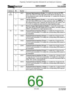
FLBK
Facility Loopback: A 1 enables the transmit line data and clock signals to
be looped back as the receive line data and clock signals.
A
TX
DS3/E3
SDH/SONET
BUS
L3M
D
RX
Facility Loopback
1
L3LBK
Line E3/DS3 Loopback: A 1 enables the receive line signal to be looped
back as the transmit line signal. The receive data and clock are provided at
the receive line interface.
A
TX
DS3/E3
RX
SDH/SONET
BUS
L3M
D
Line Loopback
TXC-03452B-MB
Ed. 6, April 2001
- 64 of 96 -

 ETC [ ETC ]