PRELIMINARY
PCT1789W DATA SHEET
PCT303DW FUNCTIONAL DESCRIPTION
!!
The remaining test modes require an off-hook sequence
to operate. The following sequence defines the off-hook
requirement:
Filter Selection
The PCT303D supports additional filter selections for
the receive and transmit signals. The IIR bit of register
16, when set, enables the IIR filters defined in Table 29
on page 59. This filter provides a much lower, however
non-linear, group delay than the default FIR filters.
1. Power up or reset.
2. Program clock generator to desired sample rate.
3. Enable line side by clearing PDL bit.
4. Issue off-hook
Revision Identification
5. Delay 4608/Fs to allow calibration to occur.
6. Set desired test mode.
The PCT303DW provides the system designer the
ability to determine the revision of the PCT303D and/or
the PCT303W. Register 11 identifies the revision of the
PCT303D with 4 bits named REVA. Register 13
identifies the revision of the PCT303W with 4 bits named
REVB. Table 12 shows the values for the various
revisions.
The ISOLink digital loopback mode allows the data
pump to provide a digital input test pattern on SDI and
receive that digital test pattern back on SDO. To enable
this mode, set the DL bit of register 1. In this mode, the
isolation barrier is actually being tested. The digital
stream is delivered across the isolation capacitor, C1 of
Figure 2 on page 6, to the line side device and returned
across the same barrier. Note in this mode, the 0.9 dB
attenuation and filter group delays also exist.
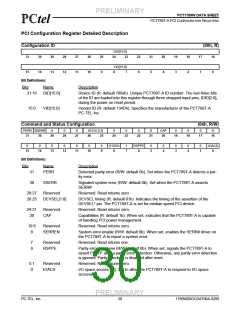
Table 12 Revision Values
Revision
PCT303D
PCT303W
A
0100
0001
The analog loopback mode allows an external device to
drive the RX pin of the line-side chip and receive the
signal from the TX pin. This mode allows testing of
external components connecting the RJ-11 jack (tip and
ring) to the line side of the PCT303DW. To enable this
mode, set the AL bit of register 2.
In-Circuit Testing
The PCT303DW’s advanced design provides the
modem manufacturer with increased ability to determine
system functionality during production line tests, as well
as support for end-user diagnostics. Four loopback
modes exist allowing increased coverage of system
components. For three of the test modes, a line-side
power source is needed. While a standard phone line
can be used, the test circuit in Figure 20 on page 60 is
adequate. In addition, an off-hook sequence must be
performed to connect the power source to the line-side
chip.
The final testing mode, internal analog loopback, allows
the system to test the basic operation of the transmit/
receive path of the line side and the external
components R4 and C5 of Figure 2 on page 6. In this
test mode, the data pump provides a digital test
waveform on SDI. This data is passed across the
isolation barrier, looped from the TX to RX pin, passed
back across the isolation barrier, and presented to the
data pump on SDO. To enable this mode, clear the HBE
bit of register 2.
For the start-up test mode, no line-side power is
necessary and no off-hook sequence is required. The
start-up test mode is enabled by default. When the PDL
bit (register 6, bit 4) is set (the default case), the line side
is in a power-down mode and the DSP side is in a digital
loop-back mode. In this mode, data received on SDI is
passed through the internal filters and transmitted on
SDO. This path will introduce approximately 0.9 dB of
attenuation on the SDI signal received. The group delay
of both transmit and receive filters will exist between SDI
and SDO. Clearing the PDL bit disables this mode and
the SDO data is switched to the receive data from the
line side. Note, when PDL is cleared the FDT bit
(register 12, bit 6) will become active, indicating the
successful communication between the line side and
DSP side. This can be used to verify that the ISOLink is
operational.
When the HBE bit is cleared, this will cause a DC offset
which affects the signal swing of the transmit signal. In
this test mode, it is recommended that the transmit
signal be 12 dB lower than normal transmit levels. This
lower level will eliminate clipping caused by the DC
offset which results from disabling the hybrid. It is
assumed in this test that the line AC impedance is
nominally 600 W.
NOTE: All test modes are mutually exclusive. If more
than one test mode is enabled concurrently, the results
are unpredictable.
PRELIMINARY
PC-TEL, Inc.
26
1789W0DOCDAT06A-0299

 ETC [ ETC ]