PRELIMINARY
PCT1789W DATA SHEET
PCT303DW FUNCTIONAL DESCRIPTION
!!
where Fs is the sample frequency, ratio is 1 for CGM=0 bypassed. Note that if M2 and N2 are set to zero, the
and 25/16 for CGM = 1, and all other symbols are shown ratio of 25/16 is eliminated and cannot be used in the
in Figure 15.
above equation. In this condition the CGM bit has no
effect.
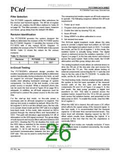
Table 11 MCLK Examples
Power Management
MCLK
(MHz)
N1
M1
CGM
The PCT303DW supports four basic power
management operation modes. The modes are normal
operation, reset operation, sleep mode, and full power
down mode. The power management modes are
controlled by the PDN and PDL bits of register 6.
1.8432
4.0000
1
5
20
72
9
0
1
0
0
1
0
1
0
1
0
0
0
0
1
0
0
0
0
1
0
0
0
1
1
4.0960
1
5.0688
11
5
80
48
6
On power up, or following a reset, the PCT303DW is in
reset operation. In this mode, the PDL bit is set, while
the PDN bit is cleared. The PCT303D is fully
operational, except for the ISOLink. No communication
between the PCT303D and PCT303W can occur during
reset operation. Note, any bits associated with the
PCT303W are not valid in this mode.
6.0000
6.1440
1
8.1920
32
1
225
4
9.2160
10.0000
10.3680
11.0592
12.288
25
9
144
32
10
3
The most common mode of operation is the normal
operation. In this mode, the PDL and PDN bits are
cleared. The PCT303D is fully operational and the
ISOLink is communicating information between the
PCT303D and the PCT303W. Note that the clock
generator must be programmed to a valid sample rate
prior to entering this mode.
3
1
14.7456
16.0000
18.4320
24.5760
25.8048
33.8688
44.2368
46.0800
47.9232
48.0000
56.0000
60.0000
2
5
5
18
2
1
The PCT303DW supports a low-power sleep mode.
This mode supports the popular wake-up-on-ring
feature of many modems. The clock generator registers
7, 8, and 9 must be programmed with valid non-zero
values prior to enabling sleep mode. Then, the PDN bit
must be set and the PDL bit cleared. When the
PCT303DW is in sleep mode, the MCLK signal may be
stopped or remain active, but it must be active before
waking up the PCT303DW. The PCT303D is non-
functional except for the ISOLink and RGDT signal. To
take the PCT303DW out of sleep mode, pulse the reset
pin (RESET) low.
2
3
7
10
160
125
4
147
96
5
13
125
35
25
10
96
36
24
In summary, the power down/up sequence for sleep
mode is as follows:
Knowing the MCLK frequency and desired sample rate
the values for the M1, N1, M2, N2 registers can be
determined. When determining these values, remember
to consider the range for each register as well as the
minimum update rate for the first PLL.
1. Registers 7, 8, and 9 must have valid non-zero
values.
2. Set the PDN bit (register 6, bit 3) and clear the PDL
bit (register 6, bit 4).
The values determined for M1, N1, M2, and N2 must be
adjusted by minus one when determining the value
3. MCLK may stay active or stop.
written to the respective registers. This is due to internal 4. Restore MCLK before initiating the power-up
logic, which adds one to the value stored in the register.
This addition allows the user to write a zero value in any
of the registers and the effective divide by is one. A
special case occurs when both M1 and N1 and/or M2
and N2 are programmed with a zero value. When Mx
and Nx are both zero, the corresponding PLLx is
sequence.
5. Reset the PCT303DW using RESET pin (after MCLK
is present).
6. Program registers to desired settings.
PRELIMINARY
PC-TEL, Inc.
24
1789W0DOCDAT06A-0299

 ETC [ ETC ]