PRELIMINARY
PCT1789W DATA SHEET
PCT303DW FUNCTIONAL DESCRIPTION
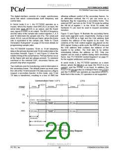
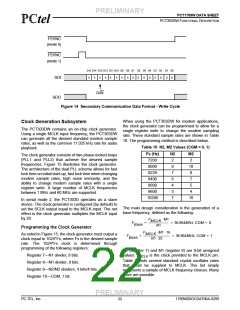
!!
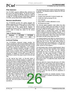
FSYNC
(mode 0)
FSYNC
(mode 1)
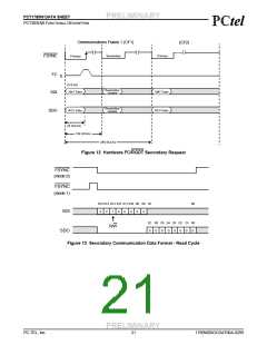
D15 D14 D13 D12 D11 D10 D9 D8 D7 D6 D5 D4 D3 D2 D1 D0
0
0
0
A
A
A
A
A
D
D
D
D
D
D
D
D
SDI
R/W
SDO
Figure 14 Secondary Communication Data Format - Write Cycle
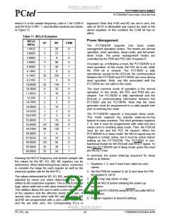
When using the PCT303DW for modem applications,
the clock generator can be programmed to allow for a
single register write to change the modem sampling
rate. These standard sample rates are shown in Table
10. The programming method is described below.
Clock Generation Subsystem
The PCT303DW contains an on-chip clock generator.
Using a single MCLK input frequency, the PCT303DW
can generate all the desired standard modem sample
rates, as well as the common 11.025 kHz rate for audio
playback.
Table 10 N2, M2 Values (CGM = 0, 1)
Fs (Hz)
7200
8000
8229
8400
9000
9600
10286
N2
2
M2
2
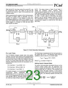
The clock generator consists of two phase-locked loops
(PLL1 and PLL2) that achieve the desired sample
frequencies. Figure 15 illustrates the clock generator.
The architecture of the dual PLL scheme allows for fast
lock time on initial start-up, fast lock time when changing
modem sample rates, high noise immunity, and the
ability to change modem sample rates with a single
register write. A large number of MCLK frequencies
between 1 MHz and 60 MHz are supported.
9
10
8
7
6
7
4
5
3
4
7
10
In serial mode 2, the PCT303D operates as a slave
device. The clock generator is configured (by default) to
set the SCLK output equal to the MCLK input. The net
effect is the clock generator multiplies the MCLK input
by 20.
The main design consideration is the generation of a
base frequency, defined as the following:
F
× M1
MCLK
= ---------------------------------- = 36.864MHz, CGM = 0
F
Base
N1
× M1 × 16
Programming the Clock Generator
F
MCLK
= --------------------------------------------- = 36.864MHz, CGM = 1
As noted in Figure 15, the clock generator must output a
clock equal to 1024*Fs, where Fs is the desired sample
rate. The 1024*Fs clock is determined through
programming of the following registers:
F
Base
N1 × 25
N1 (register 7) and M1 (register 8) are 8-bit unsigned
values. FMCLK is the clock provided to the MCLK pin.
Register 7—N1 divider, 8 bits.
Register 8—M1 divider, 8 bits.
Register 9—N2/M2 dividers, 4 bits/4 bits.
Register 10—CGM, 1 bit.
Table 11 lists several standard crystal oscillator rates
that could be supplied to MCLK. This list simply
represents a sample of MCLK frequency choices. Many
more are possible.
PRELIMINARY
PC-TEL, Inc.
22
1789W0DOCDAT06A-0299

 ETC [ ETC ]