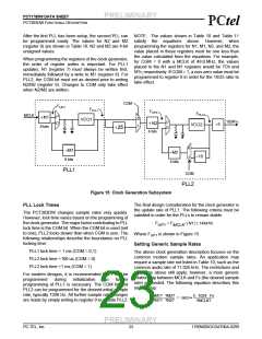
PCT1789W DATA SHEET
PRELIMINARY
PCT303DW FUNCTIONAL DESCRIPTION
!!
Exception Handling
The PCT303DW provides several mechanisms to
determine if an error occurs during operation. Through
the secondary frames of the serial link, the controlling
DSP can read several status bits. The bit of highest
importance is the frame detect bit (FDT, register 12 bit
6). This bit indicates that the DSP side (PCT303D) and
line side (PCT303W) devices are communicating.
During normal operation, the FDT bit can be checked
before reading any bits that indicate information about
the line side. If FDT is not set, the following bits related
to the line side are invalid—RDT, LCS, CBID, REVB; the
RGDT operation will also be non-functional.
Following power-up and reset, the FDT bit is not set
because the PDL bit (register 6 bit 4) defaults to 1. In this
state, the ISOLink is not operating and no information
about the line side can be determined. The user must
program the clock generator to a valid configuration for
the system and clear the PDL bit to activate the ISOLink.
While the DSP and line side are establishing
communication, the DSP side does not generate
FSYNC signals. Therefore, if the controlling DSP serial
interface is interrupt driven, based on the FSYNC signal,
the controlling DSP does not require a special delay
loop to wait for this event to complete.
The FDT bit can also indicate if the line side executes an
off-hook request successfully. If the line side is not
connected to a phone line (that is, the user fails to
connect a phone line to the modem), the FDT bit
remains cleared. The controlling DSP must allow
sufficient time for the line side to execute the off-hook
request. The maximum time for FDT to be valid following
an off-hook request is 10 ms. If the FDT is high, the LCS
bits indicate the amount of loop current flowing. If the
FDT fails to be set following an off-hook request, the
PDL bit in register 6 must be set high for at least 1 ms to
reset the line side. For more information, see “Loop
Current Monitor” on page 25.
Another useful bit is the communication link error (CLE)
bit (register 12 bit 7). The CLE bit indicates a time-out
error for the ISOLink following a change to either PLL1
or PLL2. For more information, see “Clock Generation
Subsystem” on page 22. When the CLE bit is set, the
DSP side chip has failed to receive verification from the
line side that the clock change has been accepted in an
expected period of time. This condition indicates a
severe error in programming the clock generator or
possibly a defective line-side chip.
PRELIMINARY
PC-TEL, Inc.
27
1789W0DOCDAT06A-0299

 ETC [ ETC ]