PCT1789W DATA SHEET
PRELIMINARY
PCT303DW FUNCTIONAL DESCRIPTION
!!
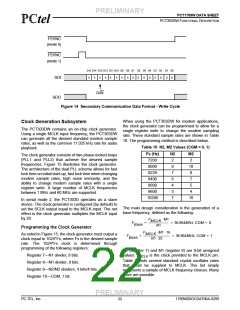
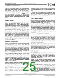
After the first PLL has been setup, the second PLL can NOTE: The values shown in Table 10 and Table 11
be programmed easily. The values for N2 and M2 satisfy the equations above. However, when
(register 9) are shown in Table 10. N2 and M2 are 4-bit programming the registers for N1, M1, N2, and M2, the
unsigned values.
value placed in these registers must be one less than
the value calculated from the equations. For example,
for CGM = 0 with a MCLK of 48.0 MHz, the values
placed in the N1 and M1 registers would be 7Ch and
5Fh, respectively. If CGM = 1, a non-zero value must be
programmed to register 9 in order for the 16/25 ratio to
take effect.
When programming the registers of the clock generator,
the order of register writes is important. For PLL1
updates, N1 (register 7) must always be written first,
immediately followed by a write to M1 (register 8). For
PLL2, the CGM bit must set as desired prior to writing
N2/M2 (register 9). Changes to CGM only take effect
when N2/M2 are written.
CGM
F
UP1
F
PLL1
F
UP2
F
PLL2
MCLK
P
¸ N1
0
1
VCO1
1024Fs
P
D
D
N2
¸
¸ 5
VCO2
8 bits
¸ 25
4 bits
0
1
¸ M1
¸ M2
¸ 16
8 bits
4 bits
PLL1
CGM
PLL2
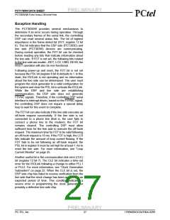
Figure 15 Clock Generation Subsystem
The final design consideration for the clock generator is
the update rate of PLL1. The following criteria must be
satisfied in order for the PLLs to remain stable:
PLL Lock Times
The PCT303DW changes sample rates very quickly.
However, lock time varies based on the programming of
the clock generator. The major factor contributing to PLL
lock time is the CGM bit. When the CGM bit is used (set
to one), PLL2 locks slower than when CGM is zero. The
following relationships describe the boundaries on PLL
locking time:
F
= F
¤ (N1 ) ³ 144kHz
UP1
MCLK
Where FUP1 is shown in Figure 15.
Setting Generic Sample Rates
PLL1 lock time < 1 ms (CGM = 0,1)
PLL2 lock time <100 us (CGM = 0)
The above clock generation description focuses on the
common modem sample rates. An application may
require a sample rate not listed in Table 10, such as the
common audio rate of 11.025 kHz. The restrictions and
equations above still apply; however, a more generic
relationship between MCLK and Fs (the desired sample
rate) is needed. The following equation describes this
relationship:
PLL2 lock time <1 ms (CGM = 1)
For modem designs, it is recommended that PLL1 be
programmed
during
initialization.
No
further
programming of PLL1 is necessary. The CGM bit and
PLL2 can be programmed for the desired initial sample
rate, typically 7200 Hz. All further sample rate changes
are made by simply writing to register 9 to update PLL2.
?M1? × ?M2?
5 ×1024 × Fs
--------------------------------- = ratio · --------------------------------
?N1? × ?N2?
?MCLK?
PRELIMINARY
PC-TEL, Inc.
23
1789W0DOCDAT06A-0299

 ETC [ ETC ]