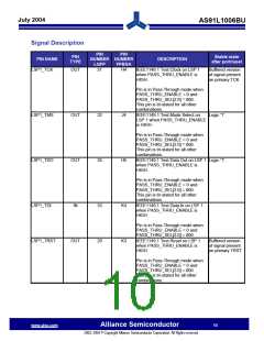
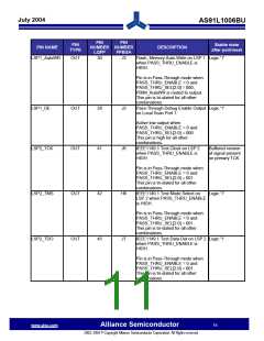
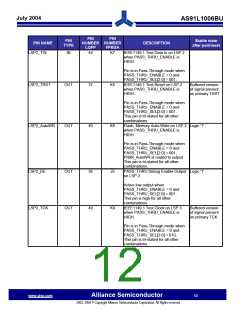
July 2004
AS91L1006BU
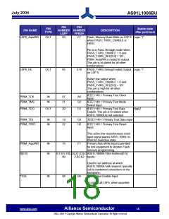
PIN
PIN
PIN
TYPE
Stable state
after port/reset
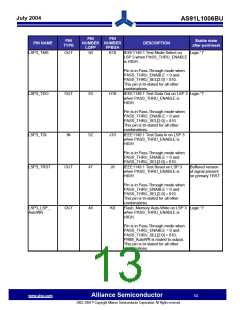
PIN NAME
LSP3_DE
NUMBER NUMBER
LQFP
DESCRIPTION
FPBGA
OUT
46
H7
PASS_THRU Debug Enable Output Logic '1'
on LSP 3.
Active low output when
PASS_THRU_ENABLE = 0 and
PASS_THRU_SEL[2:0] = 010.
This pin is high for all other
combinations.
LSP4_TCK
LSP4_TMS
LSP4_TDO
LSP4_TDI
OUT
79
78
76
77
A8
IEEE1149.1 Test Clock on LSP 4
when PASS_THRU_ENABLE is
HIGH.
Buffered version
of signal present
on primary TCK
Pin is in Pass-Through mode when
PASS_THRU_ENABLE = 0 and
PASS_THRU_SEL[2:0] = 011.
This pin is tri-stated for all other
combinations.
IEEE1149.1 Test Mode Select on
LSP 4 when PASS_THRU_ENABLE
is HIGH.
OUT
OUT
IN
A9
Logic '1'
Pin is in Pass-Through mode when
PASS_THRU_ENABLE = 0 and
PASS_THRU_SEL[2:0] = 011.
This pin is tri-stated for all other
combinations.
IEEE1149.1 Test Data Out on LSP 4 Logic '1'
when PASS_THRU_ENABLE is
HIGH.
B10
Pin is in Pass-Through mode when
PASS_THRU_ENABLE = 0 and
PASS_THRU_SEL[2:0] = 011.
This pin is tri-stated for all other
combinations.
IEEE1149.1 Test Data In on LSP 4
when PASS_THRU_ENABLE is
HIGH.
B9
Pin is in Pass-Through mode when
PASS_THRU_ENABLE = 0 and
PASS_THRU_SEL[2:0] = 011.
www.alsc.com
Alliance Semiconductor
2003, 2004 © Copyright Alliance Semiconductor Corporation. All Rights reserved.
14

 ETC [ ETC ]