July 2004
AS91L1006BU
PIN
PIN
PIN
TYPE
Stable state
after port/reset
PIN NAME
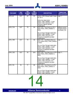
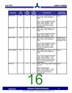
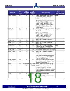
LSP6_AutoWR
NUMBER NUMBER
LQFP
DESCRIPTION
FPBGA
OUT
63
F7
Flash, Memory Auto-Write on LSP 6 Logic '1'
when PASS_THRU_ENABLE is
HIGH.
Pin is in Pass-Through mode when
PASS_THRU_ENABLE = 0 and
PASS_THRU_SEL[2:0] = 101;
PRIM_AutoWR is routed to output.
This pin is tri-stated for all other
combinations.
LSP6_DE
OUT
65
E10
PASS_THRU Debug Enable Output Logic '1'
on LSP 6.
Active low output when
PASS_THRU_ENABLE = 0 and
PASS_THRU_SEL[2:0] = 101.
This pin is high for all other
combinations.
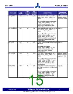
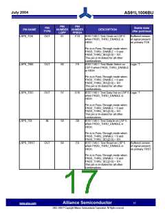
IEEE1149.1 Primary Test Clock
Input.
IEEE1149.1 Primary Test Mode
Select Input.
PRIM_TCK
PRIM_TMS
IN
IN
87
21
A6
G2
PRIM_TDO
OUT
20
G1
IEEE1149.1 Primary Test Data
Output. This pin is tri-stated when
AS91L1006BUis not selected.
HighZ
PRIM_TDI
IN
IN
19
22
G3
H2
IEEE1149.1 Primary Test Data Input
PRIM_TRST
IEEE1149.1 Primary Test Reset
Input.
This active low asynchronous reset
input signal places AS91L1006U in
Wait-for-Selection state.
PRIM_AutoWR
S[5:0]
IN
IN
16
F1
Primary Auto-Write Input controlled
by test equipment to shorten Flash
memory programming.
8,7,6,5,100, D2,D1,D3,C AS91L1006BU Slot Address[5:0]
99
2,B2,A2 Inputs.
Used to set address at which
AS91L1006BU will respond; typically
set by hardwired connection on the
backplane.
*TOE
IN
88
B6
Test Output Enable Input.
Tri-states all LSPs, when asserted
low.
www.alsc.com
Alliance Semiconductor
2003, 2004 © Copyright Alliance Semiconductor Corporation. All Rights reserved.
18

 ETC [ ETC ]