R
QPRO XQ4000E/EX QML High-Reliability FPGAs
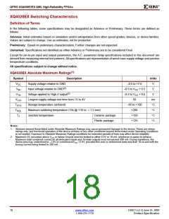
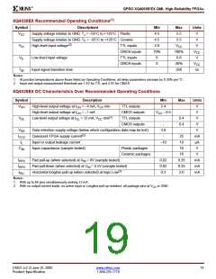
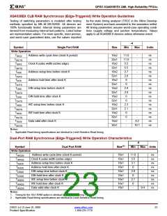
XQ4028EX Recommended Operating Conditions(1)
Symbol
Descriptiont
Min
4.5
4.5
2.0
70%
0
Max
5.5
Units
V
Supply voltage relative to GND, T = –55°C to +125°C Plastic
V
V
V
CC
J
Supply voltage relative to GND, T = –55°C to +125°C Ceramic
5.5
C
(2)
V
High-level input voltage
Low-level input voltage
Input signal transition time
TTL inputs
V
CC
IH
CMOS inputs
TTL inputs
100%
0.8
V
CC
V
V
IL
CMOS inputs
0
20%
250
V
CC
T
-
ns
IN
Notes:
1. At junction temperatures above those listed as Operating Conditions, all delay parameters increase by 0.35% per °C.
2. Input and output measurement threshold are 1.5V for TTL and 2.5V for CMOS.
XQ4028EX DC Characteristics Over Recommended Operating Conditions
Symbol
Description
Min
Max
-
Units
V
V
High-level output voltage at I
High-level output voltage at I
= –4 mA, V min
TTL outputs
2.4
OH
OH
OH
CC
= –1 mA
CMOS outputs
TTL outputs
V
– 0.5
-
V
CC
(1)
V
Low-level output voltage at I = 12 mA, V min
-
-
0.4
0.4
-
V
OL
OL
CC
CMOS outputs
V
V
Data retention supply voltage (below which configuration data may be lost)
3.0
-
V
DR
(2)
I
Quiescent FPGA supply current
25
10
10
16
0.25
0.25
2.0
mA
µA
V
CCO
I
Input or output leakage current
–10
-
L
C
Input capacitance (sample tested)
Plastic packages
IN
Ceramic packages
-
V
I
I
Pad pull-up (when selected) at V = 0V (sample tested)
0.02
0.02
0.3
mA
mA
mA
RPU
RPD
IN
Pad pull-down (when selected) at V = 5.5V (sample tested)
IN
(3)
I
Horizontal longline pull-up (when selected) at logic Low
RLL
Notes:
1. With up to 64 pins simultaneously sinking 12 mA.
2. With no output current loads, no active input or Longline pull-up resistors, all package pins at V or GND.
CC
DS021 (v2.2) June 25, 2000
www.xilinx.com
19
Product Specification
1-800-255-7778

 XILINX [ XILINX, INC ]