R
QPRO XQ4000E/EX QML High-Reliability FPGAs
XQ4028EX Switching Characteristics
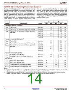
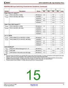
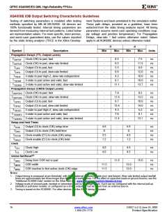
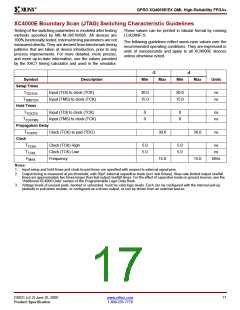
Definition of Terms
In the following tables, some specifications may be designated as Advance or Preliminary. These terms are defined as
follows:
Advance: Initial estimates based on simulation and/or extrapolation from other speed grades, devices, or device families.
Values are subject to change. Use as estimates, not for production.
Preliminary: Based on preliminary characterization. Further changes are not expected.
Unmarked: Specifications not identified as either Advance or Preliminary are to be considered Final.
Except for pin-to-pin input and output parameters, the A.C. parameter delay specifications included in this document are
derived from measuring internal test patterns. All specifications are representative of worst-case supply voltage and junction
temperature conditions.
All specifications subject to change without notice.
XQ4028EX Absolute Maximum Ratings(1)
Symbol
Description
Units
V
V
Supply voltage relative to GND
–0.5 to +7.0
–0.5 to V + 0.5
CC
(2)
V
Input voltage relative to GND
V
IN
TS
CC
(2)
V
Voltage applied to High-Z output
–0.5 to V + 0.5
V
CC
V
T
Longest supply voltage rise time from 1V to 4V
Storage temperature (ambient)
50
–65 to +150
+260
ms
°C
°C
°C
°C
CCt
STG
SOL
T
Maximum soldering temperature (10s @ 1/16 in. = 1.5 mm)
T
Junction temperature
Ceramic package
Plastic package
+150
J
+125
Notes:
1. Stresses beyond those listed under Absolute Maximum Ratings may cause permanent damage to the device. These are stress
ratings only, and functional operation of the device at these or any other conditions beyond those listed under Operating Conditions
is not implied. Exposure to Absolute Maximum Ratings conditions for extended periods of time may affect device reliability.
2. Maximum DC excursion above V or below Ground must be limited to either 0.5V or 10 mA, whichever is easier to achieve.
CC
Maximum total combined current on all dedicated inputs and Tri-state outputs must not exceed 200 mA. During transitions, the
device pins may undershoot to –2.0V or overshoot toV +2.0V, provided this over or undershoot lasts less than 10 ns and with the
CC
forcing current being limited to 200 mA.
18
www.xilinx.com
DS021 (v2.2) June 25, 2000
1-800-255-7778
Product Specification

 XILINX [ XILINX, INC ]