R
QPRO XQ4000E/EX QML High-Reliability FPGAs
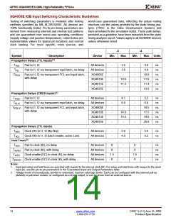
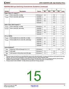
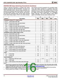
XQ4000E IOB Input Switching Characteristic Guidelines (continued)
-3
-4
Symbol
Description
Device
Min
Max
Min
Max
Units
Setup Times (TTL Inputs)(1,2)
T
Pad to clock (IK), no delay
Pad to clock (IK), with delay
All devices
XQ4005E
XQ4010E
XQ4013E
XQ4025E
2.6
-
-
-
-
-
-
4.0
-
-
-
-
-
ns
ns
ns
ns
ns
PICK
T
10.9
11.3
11.8
14.0
PICKD
9.8
10.2
-
Setup Times (CMOS Inputs)(1,2)
T
Pad to clock (IK), no delay
Pad to clock (IK), with delay
All devices
XQ4005E
XQ4010E
XQ4013E
XQ4025E
3.3
-
-
-
-
-
-
6.0
-
-
-
-
-
ns
ns
ns
ns
ns
PICKC
T
12.0
13.0
13.5
16.0
PICKDC
10.5
10.9
-
(TTL or CMOS)
T
Clock enable (EC) to clock (IK), no delay
Clock enable (EC) to clock (IK), with delay
All devices
XQ4005E
XQ4010E
XQ4013E
XQ4025E
2.5
-
-
-
-
-
-
3.5
-
-
-
-
-
ns
ns
ns
ns
ns
ECIK
T
10.4
10.7
11.1
14.0
ECIKD
9.7
10.1
-
Global Set/Reset(3)
T
Delay from GSR net through Q to I1, I2
GSR width
All devices
All devices
All devices
-
7.8
-
12.0
ns
ns
ns
RRI
T
11.5
11.5
-
-
13.0
13.0
-
-
MRW
T
GSR inactive to first active clock (IK) edge
MRI
Notes:
1. Input pad setup and hold times are specified with respect to the internal clock (IK). For setup and hold times with respect to the clock
input pin, see the pin-to-pin parameters in the Guaranteed Input and Output Parameters table.
2. Voltage levels of unused pads, bonded or unbonded, must be valid logic levels. Each can be configured with the internal pull-up
(default) or pull-down resistor, or configured as a driven output, or can be driven from an external source.
3. Timing is based on the XC4005E. For other devices see the XACT timing calculator.
DS021 (v2.2) June 25, 2000
www.xilinx.com
15
Product Specification
1-800-255-7778

 XILINX [ XILINX, INC ]