R
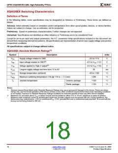
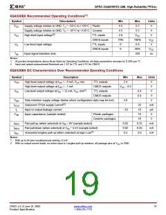
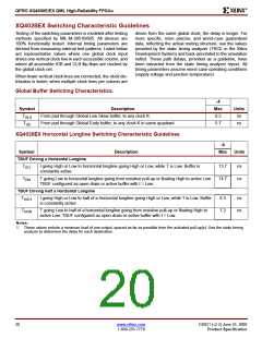
QPRO XQ4000E/EX QML High-Reliability FPGAs
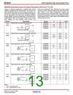
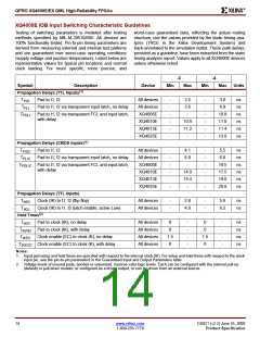
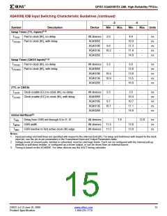
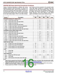
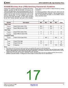
XC4000E Boundary Scan (JTAG) Switching Characteristic Guidelines
Testing of the switching parameters is modeled after testing
methods specified by MIL-M-38510/605. All devices are
100% functionally tested. Internal timing parameters are not
measured directly. They are derived from benchmark timing
patterns that are taken at device introduction, prior to any
process improvements. For more detailed, more precise,
and more up-to-date information, use the values provided
by the XACT timing calculator and used in the simulator.
These values can be printed in tabular format by running
LCA2XNF-S.
The following guidelines reflect worst-case values over the
recommended operating conditions. They are expressed in
units of nanoseconds and apply to all XC4000E devices
unless otherwise noted.
-3
-4
Symbol
Description
Min
Max
Min
Max
Units
Setup Times
T
Input (TDI) to clock (TCK)
30.0
15.0
30.0
15.0
ns
ns
TDITCK
T
Input (TMS) to clock (TCK)
TMSTCK
Hold Times
T
Input (TDI) to clock (TCK)
Input (TMS) to clock (TCK)
0
0
0
0
ns
ns
TCKTDI
T
TCKTMS
Propagation Delay
T
Clock (TCK) to pad (TDO)
30.0
15.0
30.0
15.0
ns
TCKPO
Clock
T
Clock (TCK) High
Clock (TCK) Low
Frequency
5.0
5.0
5.0
5.0
ns
ns
TCKH
T
TCKL
F
MHz
MAX
Notes:
1. Input setup and hold times and clock-to-pad times are specified with respect to external signal pins.
2. Output timing is measured at pin threshold, with 50pF external capacitive loads (incl. test fixture). Slew-rate limited output rise/fall
times are approximately two times longer than fast output rise/fall times. For the effect of capacitive loads on ground bounce, see the
“Additional XC4000 Data” section of the Programmable Logic Data Book.
3. Voltage levels of unused pads, bonded or unbonded, must be valid logic levels. Each can be configured with the internal pull-up
(default) or pull-down resistor, or configured as a driven output, or can be driven from an external source.
DS021 (v2.2) June 25, 2000
www.xilinx.com
17
Product Specification
1-800-255-7778

 XILINX [ XILINX, INC ]