R
QPRO XQ4000E/EX QML High-Reliability FPGAs
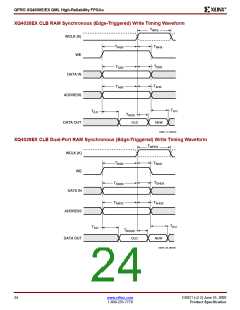
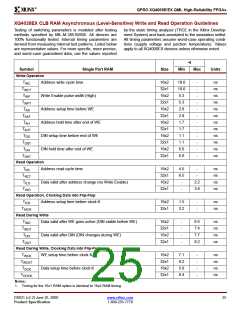
XQ4028EX CLB RAM Synchronous (Edge-Triggered) Write Operation Guidelines
Testing of switching parameters is modeled after testing
methods specified by MIL-M-38510/605. All devices are
100% functionally tested. Internal timing parameters are
derived from measuring internal test patterns. Listed below
are representative values. For more specific, more precise,
and worst-case guaranteed data, use the values reported
by the static timing analyzer (TRCE in the Xilinx Develop-
ment System) and back-annotated to the simulation netlist.
All timing parameters assume worst-case operating condi-
tions (supply voltage and junction temperature). Values
apply to all XQ4000EX devices unless otherwise noted.
-4
Symbol
Single Port RAM
Size
Min
Max
Units
Write Operation
T
Address write cycle time (clock K period)
Clock K pulse width (active edge)
Address setup time before clock K
Address hold time after clock K
DIN setup time before clock K
DIN hold time after clock K
16x2
32x1
16x2
32x1
16x2
32x1
16x2
32x1
16x2
32x1
16x2
32x1
16x2
32x1
16x2
32x1
16x2
32x1
11.0
11.0
5.5
5.5
2.7
2.6
0
-
ns
ns
ns
ns
ns
ns
ns
ns
ns
ns
ns
ns
ns
ns
ns
ns
ns
ns
WCS
T
-
WCTS
T
-
WPS
T
-
WPTS
T
-
ASS
T
-
ASTS
T
-
AHS
T
0
-
AHTS
T
2.4
2.9
0
-
DSS
T
-
DSTS
T
-
DHS
T
0
-
DHTS
T
WE setup time before clock K
WE hold time after clock K
2.3
2.1
0
-
WSS
T
T
T
-
-
WSTS
T
WHS
0
-
WHTS
T
Data valid after clock K
-
8.2
10.1
WOS
-
WOTS
Notes:
1. Applicable Read timing specifications are identical to Level-Sensitive Read timing.
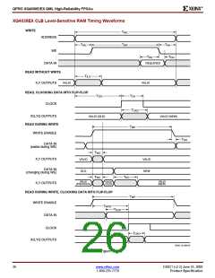
Dual-Port RAM Synchronous (Edge-Triggered) Write Operation Characteristics
-4
(1)
Symbol
Dual Port RAM
Size
Min
Max Units
Write Operation
T
T
Address write cycle time (clock K period)
Clock K pulse width (active edge)
Address setup time before clock K
Address hold time after clock K
DIN setup time before clock K
DIN hold time after clock K
16x1
16x1
16x1
16x1
16x1
16x1
16x1
16x1
16x1
11.0
5.5
3.1
0
ns
WCDS
WPDS
-
ns
ns
ns
ns
ns
ns
ns
ns
T
-
ASDS
T
-
AHDS
T
T
2.9
0
-
DSDS
DHDS
WSDS
WHDS
WODS
-
-
T
T
T
WE setup time before clock K
WE hold time after clock K
2.1
0
-
Data valid after clock K
-
9.4
Notes:
1. Timing for the 16x1 RAM option is identical to 16x2 RAM timing.
2. Applicable Read timing specifications are identical to Level-Sensitive Read timing.
DS021 (v2.2) June 25, 2000
www.xilinx.com
23
Product Specification
1-800-255-7778

 XILINX [ XILINX, INC ]