R
QPRO XQ4000E/EX QML High-Reliability FPGAs
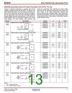
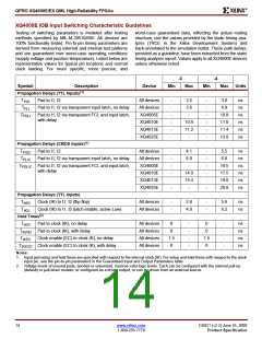
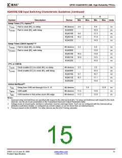
XQ4000E IOB Input Switching Characteristic Guidelines
Testing of switching parameters is modeled after testing
methods specified by MIL-M-38510/605. All devices are
100% functionally tested. Pin-to-pin timing parameters are
derived from measuring external and internal test patterns
and are guaranteed over worst-case operating conditions
(supply voltage and junction temperature). Listed below are
representative values for typical pin locations and normal
clock loading. For more specific, more precise, and
worst-case guaranteed data, reflecting the actual routing
structure, use the values provided by the static timing ana-
lyzer (TRCE in the Xilinx Development System) and
back-annotated to the simulation netlist. These path delays,
provided as a guideline, have been extracted from the static
timing analyzer report. Values apply to all XQ4000E devices
unless otherwise noted.
-3
-4
Symbol
Description
Device
Min
Max
Min
Max
Units
Propagation Delays (TTL Inputs)(1)
T
Pad to I1, I2
All devices
All devices
XQ4005E
XQ4010E
XQ4013E
XQ4025E
-
-
-
-
-
-
2.5
3.6
-
-
-
-
-
-
-
3.0
4.8
ns
ns
ns
ns
ns
ns
PID
T
Pad to I1, I2 via transparent input latch, no delay
PLI
T
Pad to I1, I2 via transparent FCL and input latch,
with delay
10.8
11.0
11.4
13.8
PDLI
10.8
11.2
-
Propagation Delays (CMOS Inputs)(1)
T
Pad to I1, I2
All devices
All devices
XQ4005E
XQ4010E
XQ4013E
XQ4025E
-
-
-
-
-
-
4.1
8.8
-
-
-
-
-
-
-
5.5
6.8
ns
ns
ns
ns
ns
ns
PIDC
T
Pad to I1, I2 via transparent input latch, no delay
PLIC
T
Pad to I1, I2 via transparent FCL and input latch,
with delay
16.5
17.5
18.0
20.8
PDLIC
14.0
14.4
-
Propagation Delays (TTL Inputs)
T
Clock (IK) to I1, I2 (flip-flop)
All devices
All devices
-
-
2.8
4.0
-
-
5.6
6.2
ns
ns
IKRI
T
Clock (IK) to I1, I2 (latch enable, active Low)
IKLI
Hold Times(2)
T
Pad to clock (IK), no delay
All devices
All devices
All devices
All devices
0
0
-
-
-
-
0
0
-
-
-
-
ns
ns
ns
ns
IKPI
T
Pad to clock (IK), with delay
IKPID
T
Clock enable (EC) to clock (K), no delay
Clock enable (EC) to clock (K), with delay
1.5
0
1.5
0
IKEC
T
IKECD
Notes:
1. Input pad setup and hold times are specified with respect to the internal clock (IK). For setup and hold times with respect to the clock
input pin, see the pin-to-pin parameters in the Guaranteed Input and Output Parameters table.
2. Voltage levels of unused pads, bonded or unbonded, must be valid logic levels. Each can be configured with the internal pull-up
(default) or pull-down resistor, or configured as a driven output, or can be driven from an external source.
14
www.xilinx.com
DS021 (v2.2) June 25, 2000
1-800-255-7778
Product Specification

 XILINX [ XILINX, INC ]