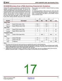
R
QPRO XQ4000E/EX QML High-Reliability FPGAs
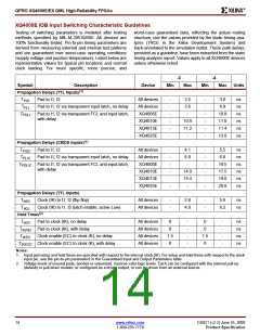
XQ4000E Guaranteed Input and Output Parameters (Pin-to-Pin, TTL I/O)
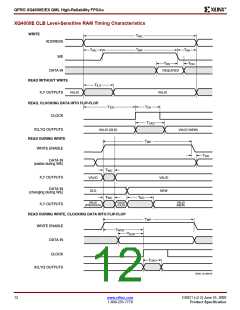
Testing of switching parameters is modeled after testing
methods specified by MIL-M-38510/605. All devices are
100% functionally tested. Pin-to-pin timing parameters are
derived from measuring external and internal test patterns
and are guaranteed over worst-case operating conditions
(supply voltage and junction temperature). Listed below are
representative values for typical pin locations and normal
clock loading. For more specific, more precise, and
worst-case guaranteed data, reflecting the actual routing
structure, use the values provided by the static timing ana-
lyzer (TRCE in the Xilinx Development System) and
back-annotated to the simulation netlist. These path delays,
provided as a guideline, have been extracted from the static
timing analyzer report. Values apply to all XQ4000E devices
unless otherwise noted.
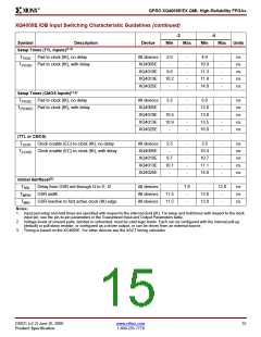
Symbol
Description
Device
-3
-
-4
Units
ns
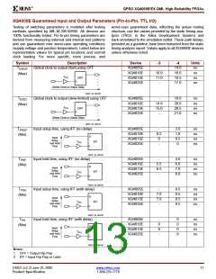
T
Global clock to output (fast) using OFF
XQ4005E
XQ4010E
XQ4013E
XQ4025E
14.0
16.0
16.5
17.0
ICKOF
10.9
11.0
-
ns
(Max)
TPG
OFF
ns
ns
Global Clock-to-Output Delay
DS021_04_060100
T
Global clock to output (slew-limited) using OFF
XQ4005E
XQ4010E
XQ4013E
XQ4025E
-
18.0
20.0
20.5
21.0
ns
ns
ns
ns
ICKO
14.9
15.0
-
(Max)
TPG
OFF
Global Clock-to-Output Delay
DS021_04_060100
T
Input setup time, using IFF (no delay)
XQ4005E
XQ4010E
XQ4013E
XQ4025E
-
0.2
0
2.0
1.0
0.5
0
ns
ns
ns
ns
PSUF
(Min)
D
Input
Setup
and Hold
Time
IFF
TPG
-
DS021_05_060100
T
Input hold time, using IFF (no delay)
XQ4005E
XQ4010E
XQ4013E
XQ4025E
-
4.6
6.0
7.0
8.0
ns
ns
ns
ns
PHF
5.5
6.5
-
(Min)
D
Input
Setup
IFF
TPG
and Hold
Time
DS021_05_060100
T
Input setup time, using IFF (with delay)
XQ4005E
XQ4010E
XQ4013E
XQ4025E
-
8.5
8.5
8.5
9.5
ns
ns
ns
ns
PSU
7.0
7.0
-
(Min)
D
Input
Setup
and Hold
Time
IFF
TPG
DS021_05_060100
T
Input hold time, using IFF (with delay)
XQ4005E
XQ4010E
XQ4013E
XQ4025E
-
0
0
-
0
0
0
0
ns
ns
ns
ns
PH
(Min)
D
Input
Setup
and Hold
IFF
TPG
Time
DS021_05_060100
Notes:
1. OFF = Output Flip-Flop
2. IFF = Input Flip-Flop or Latch
DS021 (v2.2) June 25, 2000
Product Specification
www.xilinx.com
1-800-255-7778
13

 XILINX [ XILINX, INC ]