R
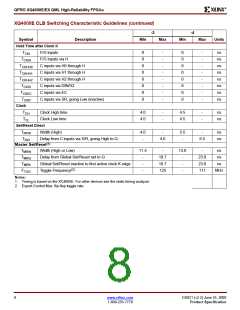
QPRO XQ4000E/EX QML High-Reliability FPGAs
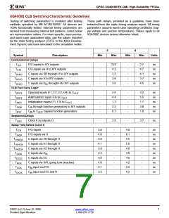
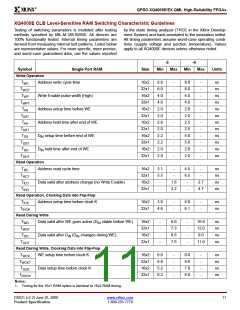
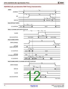
XQ4000E CLB Level-Sensitive RAM Switching Characteristic Guidelines
Testing of switching parameters is modeled after testing
methods specified by MIL-M-38510/605. All devices are
100% functionally tested. Internal timing parameters are
derived from measuring internal test patterns. Listed below
are representative values. For more specific, more precise,
and worst-case guaranteed data, use the values reported
by the static timing analyzer (TRCE in the Xilinx Develop-
ment System) and back-annotated to the simulation netlist.
All timing parameters assume worst-case operating condi-
tions (supply voltage and junction temperature). Values
apply to all XQ4000E devices unless otherwise noted.
-3
-4
Symbol
Single Port RAM
Size
Min
Max
Min
Max
Units
Write Operation
T
Address write cycle time
16x2
32x1
16x2
32x1
16x2
32x1
16x2
32x1
16x2
32x1
16x2
32x1
8.0
8.0
4.0
4.0
2.0
2.0
2.0
2.0
2.2
2.2
2.0
2.0
-
-
-
-
-
-
-
-
-
-
-
-
8.0
8.0
4.0
4.0
2.0
2.0
2.5
2.0
4.0
5.0
2.0
2.0
-
-
-
-
-
-
-
-
-
-
-
-
ns
ns
ns
ns
ns
ns
ns
ns
ns
ns
ns
ns
WC
T
WCT
T
Write Enable pulse width (High)
Address setup time before WE
Address hold time after end of WE
WP
T
WPT
T
AS
T
AST
T
AH
T
AHT
T
D
D
setup time before end of WE
hold time after end of WE
DS
IN
IN
T
T
DST
T
DH
DHT
Read Operation
T
Address read cycle time
16x2
32x1
16x2
32x1
3.1
5.5
-
-
4.5
6.5
-
-
ns
ns
ns
ns
RC
T
-
-
RCT
T
Data valid after address change (no Write Enable)
1.8
3.2
2.7
4.7
ILO
T
-
-
IHO
Read Operation, Clocking Data into Flip-Flop
Address setup time before clock K
T
16x2
32x1
3.0
4.6
-
-
4.0
6.1
-
-
ns
ns
ICK
T
IHCK
Read During Write
Data valid after WE goes active (D stable before WE)
T
16x2
32x1
16x2
32x1
-
-
-
-
6.0
7.3
6.6
7.6
-
-
-
-
10.0
12.0
9.0
ns
ns
ns
ns
WO
IN
T
WOT
T
Data valid after D (D changes during WE)
IN IN
DO
T
11.0
DOT
Read During Write, Clocking Data into Flip-Flop
T
WE setup time before clock K
16x2
32x1
16x2
32x1
6.0
6.8
5.2
6.2
-
-
-
-
8.0
9.6
7.0
8.0
-
-
-
-
ns
ns
ns
ns
WCK
T
WCKT
T
Data setup time before clock K
DCK
T
DOCK
Notes:
1. Timing for the 16x1 RAM option is identical to 16x2 RAM timing.
DS021 (v2.2) June 25, 2000
Product Specification
www.xilinx.com
1-800-255-7778
11

 XILINX [ XILINX, INC ]