R
Spartan-II FPGA Family: DC and Switching Characteristics
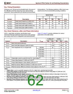
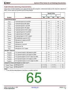
DLL Timing Parameters
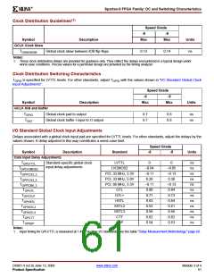
All devices are 100 percent functionally tested. Because of
the difficulty in directly measuring many internal timing
parameters, those parameters are derived from benchmark
timing patterns. The following guidelines reflect worst-case
values across the recommended operating conditions.
Speed Grade
-6
-5
Symbol
FCLKINHF
FCLKINLF
TDLLPWHF
TDLLPWLF
Description
Min
60
Max
200
100
-
Min
60
Max
180
90
-
Units
MHz
MHz
ns
Input clock frequency (CLKDLLHF)
Input clock frequency (CLKDLL)
Input clock pulse width (CLKDLLHF)
Input clock pulse width (CLKDLL)
25
25
2.0
2.5
2.4
3.0
-
-
ns
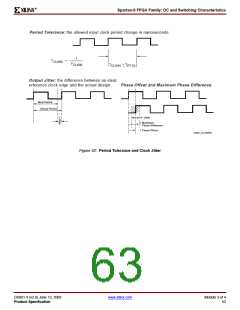
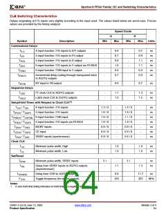
DLL Clock Tolerance, Jitter, and Phase Information
All DLL output jitter and phase specifications were
determined through statistical measurement at the package
pins using a clock mirror configuration and matched drivers.
Figure 52, page 63, provides definitions for various
parameters in the table below.
CLKDLLHF
CLKDLL
Min Max
Symbol
TIPTOL
TIJITCC
TLOCK
Description
FCLKIN
Min
Max
1.0
±150
20
Units
ns
Input clock period tolerance
-
-
-
-
-
-
-
-
-
-
-
-
-
-
-
-
-
-
-
-
-
-
-
-
1.0
±300
20
Input clock jitter tolerance (cycle-to-cycle)
Time required for DLL to acquire lock
ps
> 60 MHz
50-60 MHz
40-50 MHz
30-40 MHz
25-30 MHz
μs
μs
μs
μs
μs
ps
-
25
-
50
-
90
-
120
±60
±100
±140
±160
±200
TOJITCC
TPHIO
TPHOO
TPHIOM
Output jitter (cycle-to-cycle) for any DLL clock output(1)
Phase offset between CLKIN and CLKO(2)
±60
±100
±140
±160
±200
ps
Phase offset between clock outputs on the DLL(3)
Maximum phase difference between CLKIN and CLKO(4)
ps
ps
TPHOOM Maximum phase difference between clock outputs on the DLL(5)
ps
Notes:
1. Output Jitter is cycle-to-cycle jitter measured on the DLL output clock, excluding input clock jitter.
2. Phase Offset between CLKIN and CLKO is the worst-case fixed time difference between rising edges of CLKIN and CLKO,
excluding output jitter and input clock jitter.
3. Phase Offset between Clock Outputs on the DLL is the worst-case fixed time difference between rising edges of any two DLL
outputs, excluding Output Jitter and input clock jitter.
4. Maximum Phase Difference between CLKIN an CLKO is the sum of Output Jitter and Phase Offset between CLKIN and CLKO,
or the greatest difference between CLKIN and CLKO rising edges due to DLL alone (excluding input clock jitter).
5. Maximum Phase Difference between Clock Outputs on the DLL is the sum of Output JItter and Phase Offset between any DLL
clock outputs, or the greatest difference between any two DLL output rising edges due to DLL alone (excluding input clock jitter).
DS001-3 (v2.8) June 13, 2008
Product Specification
www.xilinx.com
Module 3 of 4
62

 XILINX [ XILINX, INC ]