R
Spartan-II FPGA Family: DC and Switching Characteristics
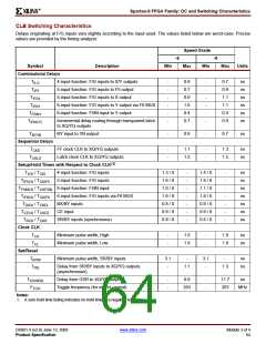
CLB Switching Characteristics
Delays originating at F/G inputs vary slightly according to the input used. The values listed below are worst-case. Precise
values are provided by the timing analyzer.
Speed Grade
-6
-5
Symbol
Description
Min
Max
Min
Max
Units
Combinatorial Delays
TILO
TIF5
4-input function: F/G inputs to X/Y outputs
5-input function: F/G inputs to F5 output
5-input function: F/G inputs to X output
6-input function: F/G inputs to Y output via F6 MUX
6-input function: F5IN input to Y output
-
-
-
-
-
-
0.6
0.7
0.9
1.0
0.4
0.7
-
-
-
-
-
-
0.7
0.9
1.1
1.1
0.4
0.9
ns
ns
ns
ns
ns
ns
TIF5X
TIF6Y
TF5INY
TIFNCTL
Incremental delay routing through transparent latch
to XQ/YQ outputs
TBYYB
Sequential Delays
TCKO
BY input to YB output
-
0.6
-
0.7
ns
FF clock CLK to XQ/YQ outputs
Latch clock CLK to XQ/YQ outputs
-
-
1.1
1.2
-
-
1.3
1.5
ns
ns
TCKLO
Setup/Hold Times with Respect to Clock CLK(1)
TICK / TCKI
4-input function: F/G inputs
5-input function: F/G inputs
1.3 / 0
1.6 / 0
1.0 / 0
1.6 / 0
0.8 / 0
0.9 / 0
0.8 / 0
-
-
-
-
-
-
-
1.4 / 0
1.8 / 0
1.1 / 0
1.8 / 0
0.8 / 0
0.9 / 0
0.8 / 0
-
-
-
-
-
-
-
ns
ns
ns
ns
ns
ns
ns
T
IF5CK / TCKIF5
T
F5INCK / TCKF5IN 6-input function: F5IN input
T
IF6CK / TCKIF6
6-input function: F/G inputs via F6 MUX
BX/BY inputs
T
DICK / TCKDI
T
CECK / TCKCE
CE input
T
RCK / TCKR
SR/BY inputs (synchronous)
Clock CLK
TCH
Minimum pulse width, High
Minimum pulse width, Low
-
-
1.9
1.9
-
-
1.9
1.9
ns
ns
TCL
Set/Reset
TRPW
Minimum pulse width, SR/BY inputs
3.1
-
-
3.1
-
-
ns
ns
TRQ
Delay from SR/BY inputs to XQ/YQ outputs
(asynchronous)
1.1
1.3
TIOGSRQ
FTOG
Delay from GSR to XQ/YQ outputs
Toggle frequency (for export control)
-
-
9.9
-
-
11.7
263
ns
263
MHz
Notes:
1. A zero hold time listing indicates no hold time or a negative hold time.
DS001-3 (v2.8) June 13, 2008
Product Specification
www.xilinx.com
Module 3 of 4
64

 XILINX [ XILINX, INC ]