R
Spartan-II FPGA Family: DC and Switching Characteristics
(1)
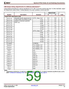
IOB Output Delay Adjustments for Different Standards
Output delays terminating at a pad are specified for LVTTL with 12 mA drive and fast slew rate. For other standards, adjust
the delays by the values shown. A delay adjusted in this way constitutes a worst-case limit.
Speed Grade
Symbol
Description
Standard
-6
-5
Units
Output Delay Adjustments (Adj)
TOLVTTL_S2
TOLVTTL_S4
TOLVTTL_S6
TOLVTTL_S8
TOLVTTL_S12
TOLVTTL_S16
TOLVTTL_S24
TOLVTTL_F2
TOLVTTL_F4
TOLVTTL_F6
TOLVTTL_F8
TOLVTTL_F12
TOLVTTL_F16
TOLVTTL_F24
TOLVCMOS2
TOPCI33_3
TOPCI33_5
TOPCI66_3
TOGTL
Standard-specific adjustments for LVTTL, Slow, 2 mA
14.2
7.2
16.9
8.6
ns
ns
ns
ns
ns
ns
ns
ns
ns
ns
ns
ns
ns
ns
ns
ns
ns
ns
ns
ns
ns
ns
ns
ns
ns
ns
ns
ns
ns
output delays terminating at pads
4 mA
(based on standard capacitive
6 mA
4.7
5.5
load, CSL
)
8 mA
2.9
3.5
12 mA
16 mA
24 mA
1.9
2.2
1.7
2.0
1.3
1.5
LVTTL, Fast, 2 mA
12.6
5.1
15.0
6.1
4 mA
6 mA
3.0
3.6
8 mA
1.0
1.2
12 mA
16 mA
24 mA
0
0
–0.1
–0.1
0.2
–0.1
–0.2
0.2
LVCMOS2
PCI, 33 MHz, 3.3V
PCI, 33 MHz, 5.0V
PCI, 66 MHz, 3.3V
GTL
2.4
2.9
2.9
3.5
–0.3
0.6
–0.4
0.7
TOGTLP
GTL+
0.9
1.1
TOHSTL_I
HSTL I
–0.4
–0.8
–0.9
–0.4
–0.8
–0.4
–0.9
–0.5
–0.8
–0.5
–1.0
–1.1
–0.5
–1.0
–0.5
–1.1
–0.6
–1.0
TOHSTL_III
TOHSTL_IV
TOSSTL2_I
TOSSLT2_II
TOSSTL3_I
TOSSTL3_II
TOCTT
HSTL III
HSTL IV
SSTL2 I
SSTL2 II
SSTL3 I
SSTL3 II
CTT
TOAGP
AGP
Notes:
1. Output timing is measured at 1.4V with 35 pF external capacitive load for LVTTL. For other I/O standards and different loads, see the
tables "Constants for Calculating TIOOP" and "Delay Measurement Methodology," page 60.
DS001-3 (v2.8) June 13, 2008
Product Specification
www.xilinx.com
Module 3 of 4
59

 XILINX [ XILINX, INC ]