R
Spartan-II FPGA Family: DC and Switching Characteristics
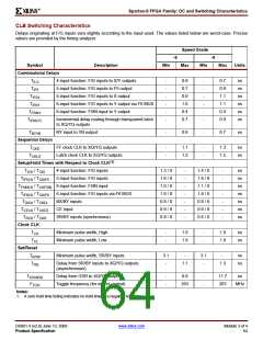
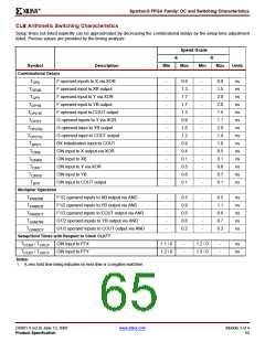
CLB Arithmetic Switching Characteristics
Setup times not listed explicitly can be approximated by decreasing the combinatorial delays by the setup time adjustment
listed. Precise values are provided by the timing analyzer.
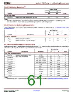
Speed Grade
-6
-5
Symbol
Description
Min
Max
Min
Max
Units
Combinatorial Delays
TOPX
TOPXB
F operand inputs to X via XOR
F operand input to XB output
F operand input to Y via XOR
F operand input to YB output
F operand input to COUT output
G operand inputs to Y via XOR
G operand input to YB output
G operand input to COUT output
BX initialization input to COUT
CIN input to X output via XOR
CIN input to XB
-
-
-
-
-
-
-
-
-
-
-
-
-
-
0.8
1.3
1.7
1.7
1.3
0.9
1.6
1.2
0.9
0.4
0.1
0.5
0.6
0.1
-
-
-
-
-
-
-
-
-
-
-
-
-
-
0.9
1.5
2.0
2.0
1.5
1.1
2.0
1.4
1.0
0.5
0.1
0.6
0.7
0.1
ns
ns
ns
ns
ns
ns
ns
ns
ns
ns
ns
ns
ns
ns
TOPY
TOPYB
TOPCYF
TOPGY
TOPGYB
TOPCYG
TBXCY
TCINX
TCINXB
TCINY
CIN input to Y via XOR
TCINYB
CIN input to YB
TBYP
CIN input to COUT output
Multiplier Operation
TFANDXB
TFANDYB
TFANDCY
TGANDYB
TGANDCY
F1/2 operand inputs to XB output via AND
F1/2 operand inputs to YB output via AND
F1/2 operand inputs to COUT output via AND
G1/2 operand inputs to YB output via AND
G1/2 operand inputs to COUT output via AND
-
-
-
-
-
0.5
0.9
0.5
0.6
0.2
-
-
-
-
-
0.5
1.1
0.6
0.7
0.2
ns
ns
ns
ns
ns
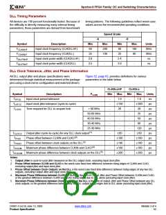
Setup/Hold Times with Respect to Clock CLK(1)
TCCKX / TCKCX
CCKY / TCKCY
Notes:
CIN input to FFX
CIN input to FFY
1.1 / 0
1.2 / 0
-
-
1.2 / 0
1.3 / 0
-
-
ns
ns
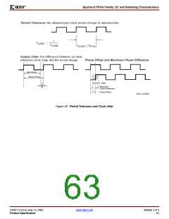
T
1. A zero hold time listing indicates no hold time or a negative hold time.
DS001-3 (v2.8) June 13, 2008
Product Specification
www.xilinx.com
Module 3 of 4
65

 XILINX [ XILINX, INC ]