R
Spartan-II FPGA Family: DC and Switching Characteristics
Speed Grade
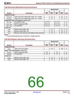
CLB Distributed RAM Switching Characteristics
-6
-5
Symbol
Sequential Delays
TSHCKO16
Description
Min
Max
Min
Max
Units
Clock CLK to X/Y outputs (WE active, 16 x 1 mode)
Clock CLK to X/Y outputs (WE active, 32 x 1 mode)
-
-
2.2
2.5
-
-
2.6
3.0
ns
ns
TSHCKO32
Setup/Hold Times with Respect to Clock CLK(1)
TAS / TAH
DS / TDH
WS / TWH
F/G address inputs
BX/BY data inputs (DIN)
CE input (WS)
0.7 / 0
0.8 / 0
0.9 / 0
-
-
-
0.7 / 0
0.9 / 0
1.0 / 0
-
-
-
ns
ns
ns
T
T
Clock CLK
TWPH
Minimum pulse width, High
-
-
-
2.9
2.9
5.8
-
-
-
2.9
2.9
5.8
ns
ns
ns
TWPL
Minimum pulse width, Low
TWC
Minimum clock period to meet address write cycle time
Notes:
1. A zero hold time listing indicates no hold time or a negative hold time.
CLB Shift Register Switching Characteristics
Speed Grade
-6
-5
Symbol
Sequential Delays
TREG
Description
Min
Max
Min
Max
Units
Clock CLK to X/Y outputs
-
3.47
-
3.88
ns
Setup Times with Respect to Clock CLK
TSHDICK
TSHCECK
Clock CLK
TSRPH
BX/BY data inputs (DIN)
CE input (WS)
0.8
0.9
-
-
0.9
1.0
-
-
ns
ns
Minimum pulse width, High
Minimum pulse width, Low
-
-
2.9
2.9
-
-
2.9
2.9
ns
ns
TSRPL
DS001-3 (v2.8) June 13, 2008
Product Specification
www.xilinx.com
Module 3 of 4
66

 XILINX [ XILINX, INC ]