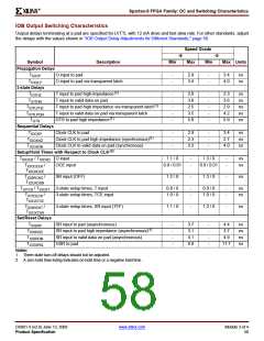
R
Spartan-II FPGA Family: DC and Switching Characteristics
(1)
Clock Distribution Guidelines
Speed Grade
-6
-5
Symbol
Description
Max
Max
Units
GCLK Clock Skew
TGSKEWIOB
Notes:
Global clock skew between IOB flip-flops
0.13
0.14
ns
1. These clock distribution delays are provided for guidance only. They reflect the delays encountered in a typical design under
worst-case conditions. Precise values for a particular design are provided by the timing analyzer.
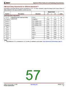
Clock Distribution Switching Characteristics
TGPIO is specified for LVTTL levels. For other standards, adjust TGPIO with the values shown in "I/O Standard Global Clock
Input Adjustments".
Speed Grade
-6
-5
Symbol
Description
Max
Max
Units
GCLK IOB and Buffer
TGPIO
TGIO
Global clock pad to output
0.7
0.7
0.8
0.8
ns
ns
Global clock buffer I input to O output
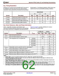
I/O Standard Global Clock Input Adjustments
Delays associated with a global clock input pad are specified for LVTTL levels. For other standards, adjust the delays by the
values shown. A delay adjusted in this way constitutes a worst-case limit.
Speed Grade
Symbol
Description
Standard
-6
-5
Units
Data Input Delay Adjustments
TGPLVTTL
TGPLVCMOS2
TGPPCI33_3
TGPPCI33_5
TGPPCI66_3
TGPGTL
Standard-specific global clock
input delay adjustments
LVTTL
LVCMOS2
PCI, 33 MHz, 3.3V
PCI, 33 MHz, 5.0V
PCI, 66 MHz, 3.3V
GTL
0
0
ns
ns
ns
ns
ns
ns
ns
ns
ns
ns
ns
ns
–0.04
–0.11
0.26
–0.11
0.80
0.71
0.63
0.52
0.56
0.62
0.54
–0.05
–0.13
0.30
–0.13
0.84
0.73
0.64
0.51
0.55
0.62
0.53
TGPGTLP
GTL+
TGPHSTL
HSTL
TGPSSTL2
TGPSSTL3
TGPCTT
SSTL2
SSTL3
CTT
TGPAGP
AGP
Notes:
1. Input timing for GPLVTTL is measured at 1.4V. For other I/O standards, see the table "Delay Measurement Methodology," page 60.
DS001-3 (v2.8) June 13, 2008
Product Specification
www.xilinx.com
Module 3 of 4
61

 XILINX [ XILINX, INC ]