R
Spartan-II FPGA Family: DC and Switching Characteristics
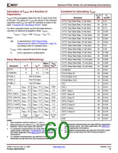
Calculation of T
Capacitance
as a Function of
Constants for Calculating T
IOOP
IOOP
(1)
CSL
FL
Standard
(pF)
35
35
35
35
35
35
35
35
35
35
35
35
35
35
35
50
10
10
0
(ns/pF)
TIOOP is the propagation delay from the O Input of the IOB
to the pad. The values for TIOOP are based on the standard
capacitive load (CSL) for each I/O standard as listed in the
table "Constants for Calculating TIOOP", below.
LVTTL Fast Slew Rate, 2 mA drive
LVTTL Fast Slew Rate, 4 mA drive
LVTTL Fast Slew Rate, 6 mA drive
LVTTL Fast Slew Rate, 8 mA drive
0.41
0.20
0.13
For other capacitive loads, use the formulas below to
calculate an adjusted propagation delay, TIOOP1
.
0.079
0.044
0.043
0.033
0.41
T
IOOP1 = TIOOP + Adj + (CLOAD – CSL) * FL
LVTTL Fast Slew Rate, 12 mA drive
LVTTL Fast Slew Rate, 16 mA drive
LVTTL Fast Slew Rate, 24 mA drive
LVTTL Slow Slew Rate, 2 mA drive
LVTTL Slow Slew Rate, 4 mA drive
LVTTL Slow Slew Rate, 6 mA drive
LVTTL Slow Slew Rate, 8 mA drive
LVTTL Slow Slew Rate, 12 mA drive
LVTTL Slow Slew Rate, 16 mA drive
LVTTL Slow Slew Rate, 24 mA drive
LVCMOS2
Where:
Adj
is selected from "IOB Output Delay
Adjustments for Different Standards", page 59,
according to the I/O standard used
0.20
CLOAD is the capacitive load for the design
FL is the capacitance scaling factor
0.100
0.086
0.058
0.050
0.048
0.041
0.050
0.050
0.033
0.014
0.017
0.022
0.016
0.014
0.028
0.016
0.029
0.016
0.035
0.037
Delay Measurement Methodology
VREF
Point Typ(2)
Meas.
(1)
(1)
Standard
LVTTL
VL
VH
0
3
1.4
-
LVCMOS2
PCI33_5
PCI33_3
PCI66_3
GTL
0
2.5
1.125
-
PCI 33 MHz 5V
Per PCI Spec
Per PCI Spec
Per PCI Spec
-
PCI 33 MHZ 3.3V
-
PCI 66 MHz 3.3V
-
GTL
V
V
V
V
REF – 0.2 VREF + 0.2 VREF
REF – 0.2 VREF + 0.2 VREF
REF – 0.5 VREF + 0.5 VREF
REF – 0.5 VREF + 0.5 VREF
0.80
1.0
0.75
0.90
0.90
1.5
1.25
1.5
GTL+
0
GTL+
HSTL Class I
20
20
20
30
30
30
30
20
10
HSTL Class I
HSTL Class III
HSTL Class III
HSTL Class IV
HSTL Class IV VREF – 0.5 VREF + 0.5 VREF
SSTL3 I and II VREF – 1.0 VREF + 1.0 VREF
SSTL2 I and II VREF – 0.75 VREF + 0.75 VREF
SSTL2 Class I
SSTL2 Class II
SSTL3 Class I
CTT
AGP
V
REF – 0.2 VREF + 0.2 VREF
VREF VREF VREF
(0.2xVCCO) (0.2xVCCO
SSTL3 Class II
–
+
Per AGP
Spec
CTT
)
AGP
Notes:
Notes:
1. Input waveform switches between VL and VH.
1. I/O parameter measurements are made with the capacitance
values shown above. See Xilinx application note XAPP179
for the appropriate terminations.
2. I/O standard measurements are reflected in the IBIS model
information except where the IBIS format precludes it.
2. Measurements are made at VREF Typ, Maximum, and
Minimum. Worst-case values are reported.
3. I/O parameter measurements are made with the capacitance
values shown in the table, "Constants for Calculating TIOOP".
See Xilinx application note XAPP179 for the appropriate
terminations.
4. I/O standard measurements are reflected in the IBIS model
information except where the IBIS format precludes it.
DS001-3 (v2.8) June 13, 2008
Product Specification
www.xilinx.com
Module 3 of 4
60

 XILINX [ XILINX, INC ]