R
Spartan-II FPGA Family: DC and Switching Characteristics
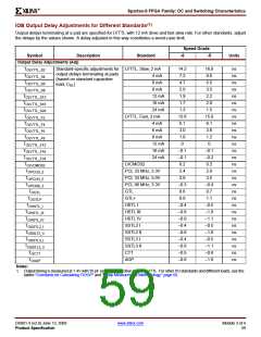
(1)
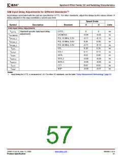
IOB Input Delay Adjustments for Different Standards
Input delays associated with the pad are specified for LVTTL. For other standards, adjust the delays by the values shown. A
delay adjusted in this way constitutes a worst-case limit.
Speed Grade
Symbol
Description
Standard
-6
-5
Units
Data Input Delay Adjustments
TILVTTL
TILVCMOS2
TIPCI33_3
TIPCI33_5
TIPCI66_3
TIGTL
Standard-specific data input delay
adjustments
LVTTL
0
0
ns
ns
ns
ns
ns
ns
ns
ns
ns
ns
ns
ns
LVCMOS2
PCI, 33 MHz, 3.3V
PCI, 33 MHz, 5.0V
PCI, 66 MHz, 3.3V
GTL
–0.04
–0.11
0.26
–0.05
–0.13
0.30
–0.11
0.20
–0.13
0.24
TIGTLP
GTL+
0.11
0.13
TIHSTL
HSTL
0.03
0.04
TISSTL2
TISSTL3
TICTT
SSTL2
–0.08
–0.04
0.02
–0.09
–0.05
0.02
SSTL3
CTT
TIAGP
AGP
–0.06
–0.07
Notes:
1. Input timing for LVTTL is measured at 1.4V. For other I/O standards, see the table "Delay Measurement Methodology," page 60.
DS001-3 (v2.8) June 13, 2008
Product Specification
www.xilinx.com
Module 3 of 4
57

 XILINX [ XILINX, INC ]