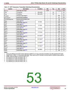
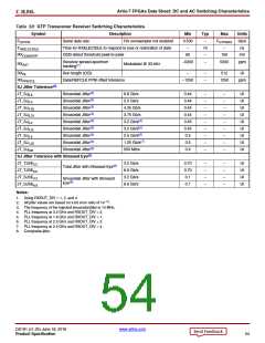
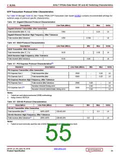
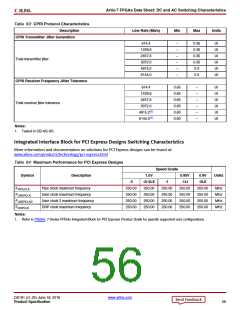
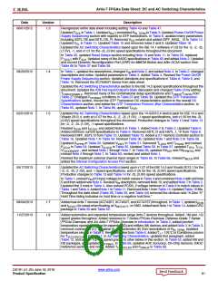
Artix-7 FPGAs Data Sheet: DC and AC Switching Characteristics
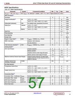
XADC Specifications
Table 65: XADC Specifications
Parameter
Symbol
Comments/Conditions
Min
Typ
Max
Units
VCCADC = 1.8V 5ꢀ, VREFP = 1.25V, VREFN = 0V, ADCCLK = 26 MHz, –55°C ≤ Tj ≤ 125°C, Typical values at Tj=+40°C
ADC Accuracy(1)
Resolution
12
–
–
–
–
–
–
–
–
–
–
–
–
–
–
3
–
–
Bits
LSBs
LSBs
LSBs
LSBs
LSBs
LSBs
ꢀ
Integral Nonlinearity(2)
INL
–40°C ≤ Tj ≤ 100°C
2
–55°C ≤ Tj < –40°C; 100°C < Tj ≤ 125°C
No missing codes, guaranteed monotonic
–40°C ≤ Tj ≤ 100°C
–
3
1
Differential Nonlinearity
Offset Error
DNL
–
Unipolar
–
8
–55°C ≤ Tj < –40°C; 100°C < Tj ≤ 125°C
–55°C ≤ Tj ≤ 125°C
–
12
4
Bipolar
–
Gain Error
–
0.5
4
Offset Matching
Gain Matching
Sample Rate
–
LSBs
ꢀ
–
0.3
1
–
MS/s
dB
Signal to Noise Ratio(2)
RMS Code Noise
SNR
THD
FSAMPLE = 500KS/s, FIN = 20 kHz
External 1.25V reference
60
–
–
2
LSBs
LSBs
dB
On-chip reference
–
–
Total Harmonic Distortion(2)
Analog Inputs(3)
FSAMPLE = 500KS/s, FIN = 20 kHz
70
–
ADC Input Ranges
Unipolar operation
0
–
–
–
–
–
1
V
V
V
V
V
Bipolar operation
–0.5
0
+0.5
Unipolar common mode range (FS input)
Bipolar common mode range (FS input)
+0.5
+0.5
–0.1
+0.6
Maximum External Channel Input Ranges
Adjacent analog channels set within these
ranges should not corrupt measurements on
adjacent channels
VCCADC
Auxiliary Channel Full
Resolution Bandwidth
FRBW
250
–
–
kHz
On-Chip Sensors
Temperature Sensor Error
–40°C ≤ Tj ≤ 100°C
–
–
–
–
–
–
–
–
4
6
1
2
°C
°C
ꢀ
–55°C ≤ Tj < –40°C; 100°C < Tj ≤ 125°C
–40°C ≤ Tj ≤ 100°C
Supply Sensor Error
–55°C ≤ Tj < –40°C; 100°C < Tj ≤ 125°C
ꢀ
Conversion Rate(4)
Conversion Time - Continuous tCONV
Number of ADCCLK cycles
Number of CLK cycles
DRP clock frequency
Derived from DCLK
26
–
–
–
–
–
–
32
21
Cycles
Cycles
MHz
MHz
ꢀ
Conversion Time - Event
DRP Clock Frequency
ADC Clock Frequency
DCLK Duty Cycle
tCONV
DCLK
8
250
26
ADCCLK
1
40
60
DS181 (v1.25) June 18, 2018
www.xilinx.com
Product Specification
57

 XILINX [ XILINX, INC ]