Artix-7 FPGAs Data Sheet: DC and AC Switching Characteristics
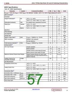
Table 65: XADC Specifications (Cont’d)
Parameter
XADC Reference(5)
External Reference
On-Chip Reference
Symbol
Comments/Conditions
Min
Typ
Max
Units
VREFP
Externally supplied reference voltage
1.20
1.25
1.30
V
V
Ground VREFP pin to AGND,
–40°C ≤ Tj ≤ 100°C
1.2375 1.25
1.2625
Ground VREFP pin to AGND,
1.225 1.25
1.275
V
–55°C ≤ Tj < –40°C; 100°C < Tj ≤ 125°C
Notes:
1. Offset and gain errors are removed by enabling the XADC automatic gain calibration feature. The values are specified for when this feature
is enabled.
2. Only specified for bitstream option XADCEnhancedLinearity = ON.
3. See the ADC chapter in the 7 Series FPGAs and Zynq-7000 AP SoC XADC Dual 12-Bit 1 MSPS Analog-to-Digital Converter (UG480) for a
detailed description.
4. See the Timing chapter in the 7 Series FPGAs and Zynq-7000 AP SoC XADC Dual 12-Bit 1 MSPS Analog-to-Digital Converter (UG480) for
a detailed description.
5. Any variation in the reference voltage from the nominal V
= 1.25V and V
= 0V will result in a deviation from the ideal transfer
REFN
REFP
function. This also impacts the accuracy of the internal sensor measurements (i.e., temperature and power supply). However, for external
ratiometric type applications allowing reference to vary by 4ꢀ is permitted.
Configuration Switching Characteristics
Table 66: Configuration Switching Characteristics
Speed Grade
Symbol
Description
1.0V
0.95V
-1LI
0.9V
-2LE
Units
-3
-2/-2LE
-1
Power-up Timing Characteristics
(1)
TPL
Program latency
5.00
10/50
10/35
250.00
5.00
10/50
10/35
250.00
5.00
10/50
10/35
250.00
5.00
10/50
10/35
250.00
5.00
ms, Max
(1)
TPOR
Power-on reset (50 ms ramp rate time)
Power-on reset (1 ms ramp rate time)
Program pulse width
10/50 ms, Min/Max
10/35 ms, Min/Max
TPROGRAM
250.00
ns, Min
CCLK Output (Master Mode)
TICCK
Master CCLK output delay
150.00
40/60
40/60
100.00
50.00
3.00
150.00
40/60
40/60
100.00
50.00
3.00
150.00
40/60
40/60
100.00
50.00
3.00
150.00
40/60
40/60
100.00
50.00
3.00
150.00
40/60
40/60
70.00
35.00
3.00
ns, Min
ꢀ, Min/Max
ꢀ, Min/Max
MHz, Max
MHz, Max
MHz, Typ
ꢀ, Max
TMCCKL
TMCCKH
FMCCK
Master CCLK clock Low time duty cycle
Master CCLK clock High time duty cycle
Master CCLK frequency
Master CCLK frequency for AES encrypted x16
FMCCK_START Master CCLK frequency at start of configuration
FMCCKTOL
Frequency tolerance, master mode with respect
to nominal CCLK
50
50
50
50
50
CCLK Input (Slave Modes)
TSCCKL
TSCCKH
FSCCK
Slave CCLK clock minimum Low time
2.50
2.50
2.50
2.50
2.50
2.50
2.50
2.50
2.50
2.50
ns, Min
ns, Min
Slave CCLK clock minimum High time
Slave CCLK frequency
100.00
100.00
100.00
100.00
70.00
MHz, Max
EMCCLK Input (Master Mode)
TEMCCKL
TEMCCKH
FEMCCK
External master CCLK Low time
2.50
2.50
2.50
2.50
2.50
2.50
2.50
2.50
2.50
2.50
ns, Min
ns, Min
External master CCLK High time
External master CCLK frequency
100.00
100.00
100.00
100.00
70.00
MHz, Max
DS181 (v1.25) June 18, 2018
www.xilinx.com
Product Specification
58

 XILINX [ XILINX, INC ]