Artix-7 FPGAs Data Sheet: DC and AC Switching Characteristics
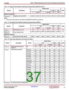
Table 36: Duty Cycle Distortion and Clock-Tree Skew (Cont’d)
Speed Grade
Symbol
Description
Device
1.0V
-2/-2LE
0.95V
-1LI
0.9V
-2LE
0.03
Units
-3
-1
-1Q/-1M
TBUFIOSKEW I/O clock tree skew across one
clock region
All
All
0.03
0.03
0.03
0.03
0.03
ns
ns
TDCD_BUFR
Regional clock tree duty cycle
distortion
0.18
0.18
0.18
0.18
0.18
0.18
Notes:
1. These parameters represent the worst-case duty cycle distortion observable at the I/O flip flops. For all I/O standards, IBIS can be used to
calculate any additional duty cycle distortion that might be caused by asymmetrical rise/fall times.
2. The T
value represents the worst-case clock-tree skew observable between sequential I/O elements. Significantly less clock-tree
CKSKEW
skew exists for I/O registers that are close to each other and fed by the same or adjacent clock-tree branches. Use the Xilinx Timing Analyzer
tools to evaluate clock skew specific to your application.
MMCM Switching Characteristics
Table 37: MMCM Specification
Speed Grade
Symbol
Description
1.0V
-2/-2LE
800.00
10.00
0.95V
-1LI
0.9V
-2LE
Units
-3
-1
MMCM_FINMAX
MMCM_FINMIN
MMCM_FINJITTER
MMCM_FINDUTY
Maximum input clock frequency
Minimum input clock frequency
Maximum input clock period jitter
800.00
10.00
800.00
10.00
800.00
10.00
800.00
10.00
MHz
MHz
< 20ꢀ of clock input period or 1 ns Max
Allowable input duty cycle:
10—49 MHz
25
30
35
40
25
30
35
40
25
30
35
40
25
30
35
40
25
30
35
40
ꢀ
ꢀ
ꢀ
ꢀ
Allowable input duty cycle:
50—199 MHz
Allowable input duty cycle:
200—399 MHz
Allowable input duty cycle:
400—499 MHz
Allowable input duty cycle: > 500 MHz
45
45
45
45
45
ꢀ
MMCM_FMIN_PSCLK
MMCM_FMAX_PSCLK
Minimum dynamic phase-shift clock
frequency
0.01
0.01
0.01
0.01
0.01
MHz
Maximum dynamic phase-shift clock
frequency
550.00
500.00
450.00
450.00
450.00
MHz
MMCM_FVCOMIN
MMCM_FVCOMAX
MMCM_FBANDWIDTH
Minimum MMCM VCO frequency
Maximum MMCM VCO frequency
Low MMCM bandwidth at typical(1)
High MMCM bandwidth at typical(1)
600.00
600.00
600.00
600.00
600.00
MHz
MHz
MHz
MHz
ns
1600.00 1440.00 1200.00 1200.00 1200.00
1.00
4.00
0.12
1.00
4.00
0.12
1.00
4.00
0.12
1.00
4.00
0.12
1.00
4.00
0.12
MMCM_TSTATPHAOFFSET Static phase offset of the MMCM
outputs(2)
MMCM_TOUTJITTER
MMCM_TOUTDUTY
MMCM output jitter
Note 3
MMCM output clock duty-cycle
precision(4)
0.20
0.20
0.20
0.20
0.25
ns
MMCM_TLOCKMAX
MMCM_FOUTMAX
MMCM_FOUTMIN
MMCM maximum lock time
100.00
800.00
4.69
100.00
800.00
4.69
100.00
800.00
4.69
100.00
800.00
4.69
100.00
800.00
4.69
µs
MMCM maximum output frequency
MMCM minimum output frequency(5)(6)
MHz
MHz
DS181 (v1.25) June 18, 2018
www.xilinx.com
Product Specification
38

 XILINX [ XILINX, INC ]