Artix-7 FPGAs Data Sheet: DC and AC Switching Characteristics
(1)
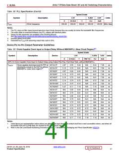
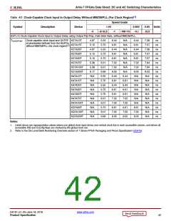
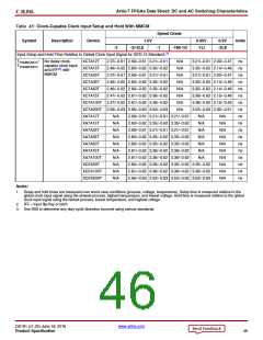
Table 40: Clock-Capable Clock Input to Output Delay Without MMCM/PLL (Far Clock Region)
Speed Grade
Symbol
Description
Device
1.0V
-2/-2LE
0.95V
-1LI
0.9V Units
-2LE
-3
-1
-1M/-1Q
SSTL15 Clock-Capable Clock Input to Output Delay using Output Flip-Flop, Fast Slew Rate, without MMCM/PLL.
TICKOFFAR Clock-capable clock input and OUTFF XC7A12T
at pins/banks farthest from the BUFGs
4.97
5.10
4.97
5.10
5.10
5.38
5.38
6.17
N/A
N/A
N/A
N/A
N/A
N/A
N/A
N/A
N/A
N/A
5.55
5.70
5.55
5.70
5.70
6.01
6.01
6.89
5.55
5.70
5.55
5.70
5.70
6.01
6.01
5.70
6.01
6.89
6.44
6.61
6.44
6.61
6.61
7.02
7.02
8.05
6.44
6.61
6.44
6.61
6.61
7.02
7.02
6.61
7.02
8.05
N/A
N/A
6.44
6.61
6.44
6.61
6.61
7.02
7.02
8.05
N/A
7.38
7.57
7.38
7.57
7.57
7.94
7.94
9.03
N/A
N/A
N/A
N/A
N/A
N/A
N/A
N/A
N/A
N/A
ns
ns
ns
ns
ns
ns
ns
ns
ns
ns
ns
ns
ns
ns
ns
ns
ns
ns
XC7A15T
without MMCM/PLL (far clock region)(2)
XC7A25T
XC7A35T
XC7A50T
XC7A75T
XC7A100T
XC7A200T
XA7A12T
XA7A15T
XA7A25T
XA7A35T
XA7A50T
XA7A75T
XA7A100T
XQ7A50T
XQ7A100T
XQ7A200T
N/A
N/A
N/A
N/A
N/A
N/A
6.44
6.61
6.44
6.61
6.61
7.02
7.02
6.61
7.02
8.05
N/A
N/A
N/A
N/A
N/A
N/A
6.61
7.02
8.05
Notes:
1. Listed above are representative values where one global clock input drives one vertical clock line in each accessible column, and where all
accessible IOB and CLB flip-flops are clocked by the global clock net.
2. Refer to the Die Level Bank Numbering Overview section of 7 Series FPGA Packaging and Pinout Specification (UG475).
DS181 (v1.25) June 18, 2018
www.xilinx.com
Product Specification
42

 XILINX [ XILINX, INC ]