Artix-7 FPGAs Data Sheet: DC and AC Switching Characteristics
Speed Grade
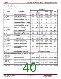
Table 38: PLL Specification (Cont’d)
Symbol
Description
1.0V
0.95V
-1LI
0.9V
-2LE
Units
-3
-2/-2LE
200.00
-1
FDCK
DCLK frequency
200.00
200.00
200.00
100.00 MHz, Max
Notes:
1. The PLL does not filter typical spread-spectrum input clocks because they are usually far below the bandwidth filter frequencies.
2. The static offset is measured between any PLL outputs with identical phase.
3. Values for this parameter are available in the Clocking Wizard.
See http://www.xilinx.com/products/intellectual-property/clocking_wizard.htm.
4. Includes global clock buffer.
5. Calculated as F
/128 assuming output duty cycle is 50ꢀ.
VCO
Device Pin-to-Pin Output Parameter Guidelines
(1)
Table 39: Clock-Capable Clock Input to Output Delay Without MMCM/PLL (Near Clock Region)
Speed Grade
Symbol
Description
Device
1.0V
-2/-2LE
0.95V
-1LI
0.9V Units
-2LE
-3
-1
-1M/-1Q
SSTL15 Clock-Capable Clock Input to Output Delay using Output Flip-Flop, Fast Slew Rate, without MMCM/PLL.
TICKOF
Clock-capable clock input and OUTFF at XC7A12T
4.97
5.10
4.97
5.10
5.10
5.14
5.14
5.47
N/A
N/A
N/A
N/A
N/A
N/A
N/A
N/A
N/A
N/A
5.55
5.70
5.55
5.70
5.70
5.74
5.74
6.11
5.55
5.70
5.55
5.70
5.70
5.74
5.74
5.70
5.74
6.11
6.44
6.61
6.44
6.61
6.61
6.72
6.72
7.16
6.44
6.61
6.44
6.61
6.61
6.72
6.72
6.61
6.72
7.16
N/A
N/A
N/A
N/A
N/A
N/A
N/A
N/A
6.44
6.61
6.44
6.61
6.61
6.72
6.72
6.61
6.72
7.16
6.44
6.61
6.44
6.61
6.61
6.72
6.72
7.16
N/A
7.38
7.56
7.38
7.56
7.56
7.62
7.62
8.08
N/A
N/A
N/A
N/A
N/A
N/A
N/A
N/A
N/A
N/A
ns
ns
ns
ns
ns
ns
ns
ns
ns
ns
ns
ns
ns
ns
ns
ns
ns
ns
pins/banks closest to the BUFGs without
XC7A15T
MMCM/PLL (near clock region)(2)
XC7A25T
XC7A35T
XC7A50T
XC7A75T
XC7A100T
XC7A200T
XA7A12T
XA7A15T
XA7A25T
XA7A35T
XA7A50T
XA7A75T
XA7A100T
XQ7A50T
XQ7A100T
XQ7A200T
N/A
N/A
N/A
N/A
N/A
N/A
6.61
6.72
7.16
Notes:
1. Listed above are representative values where one global clock input drives one vertical clock line in each accessible column, and where all
accessible IOB and CLB flip-flops are clocked by the global clock net.
2. Refer to the Die Level Bank Numbering Overview section of 7 Series FPGA Packaging and Pinout Specification (UG475).
DS181 (v1.25) June 18, 2018
www.xilinx.com
Product Specification
41

 XILINX [ XILINX, INC ]