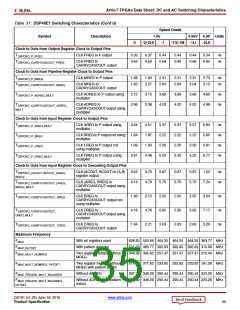
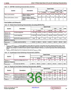
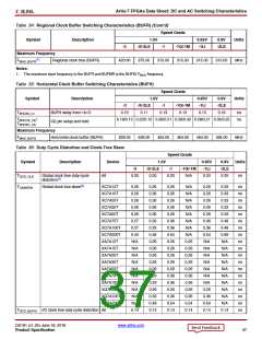
Artix-7 FPGAs Data Sheet: DC and AC Switching Characteristics
Speed Grade
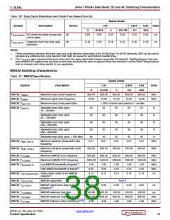
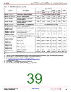
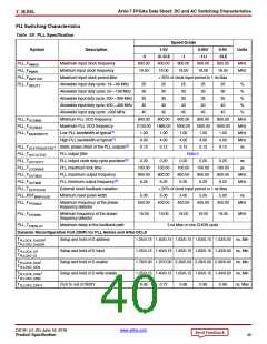
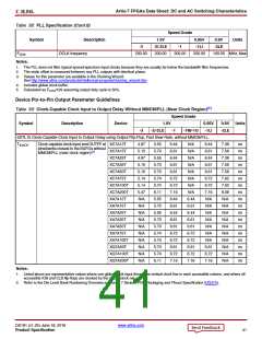
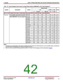
Table 37: MMCM Specification (Cont’d)
Symbol
Description
1.0V
0.95V
-1LI
0.9V
-2LE
Units
-3
-2/-2LE
-1
MMCM_TEXTFDVAR
MMCM_RSTMINPULSE
MMCM_FPFDMAX
External clock feedback variation
Minimum reset pulse width
< 20ꢀ of clock input period or 1 ns Max
5.00
5.00
5.00
5.00
5.00
ns
Maximum frequency at the phase
frequency detector
550.00
500.00
450.00
450.00
450.00
MHz
MMCM_FPFDMIN
Minimum frequency at the phase
frequency detector
10.00
10.00
10.00
10.00
10.00
MHz
MMCM_TFBDELAY
Maximum delay in the feedback path
3 ns Max or one CLKIN cycle
MMCM Switching Characteristics Setup and Hold
TMMCMDCK_PSEN
/
Setup and hold of phase-shift enable
1.04/0.00 1.04/0.00 1.04/0.00 1.04/0.00 1.04/0.00
1.04/0.00 1.04/0.00 1.04/0.00 1.04/0.00 1.04/0.00
ns
ns
ns
TMMCMCKD_PSEN
TMMCMDCK_PSINCDEC
TMMCMCKD_PSINCDEC
/
Setup and hold of phase-shift
increment/decrement
TMMCMCKO_PSDONE
Phase shift clock-to-out of PSDONE
0.59
0.68
0.81
0.81
0.78
Dynamic Reconfiguration Port (DRP) for MMCM Before and After DCLK
TMMCMDCK_DADDR
TMMCMCKD_DADDR
/
DADDR setup/hold
1.25/0.15 1.40/0.15 1.63/0.15 1.63/0.15 1.43/0.00 ns, Min
1.25/0.15 1.40/0.15 1.63/0.15 1.63/0.15 1.43/0.00 ns, Min
1.76/0.00 1.97/0.00 2.29/0.00 2.29/0.00 2.40/0.00 ns, Min
1.25/0.15 1.40/0.15 1.63/0.15 1.63/0.15 1.43/0.00 ns, Min
TMMCMDCK_DI
TMMCMCKD_DI
/
DI setup/hold
TMMCMDCK_DEN
/
DEN setup/hold
DWE setup/hold
TMMCMCKD_DEN
TMMCMDCK_DWE
/
TMMCMCKD_DWE
TMMCMCKO_DRDY
FDCK
CLK to out of DRDY
DCLK frequency
0.65
0.72
0.99
0.99
0.99
ns, Max
200.00
200.00
200.00
200.00
100.00 MHz, Max
Notes:
1. The MMCM does not filter typical spread-spectrum input clocks because they are usually far below the bandwidth filter frequencies.
2. The static offset is measured between any MMCM outputs with identical phase.
3. Values for this parameter are available in the Clocking Wizard.
See http://www.xilinx.com/products/intellectual-property/clocking_wizard.htm.
4. Includes global clock buffer.
5. Calculated as F
/128 assuming output duty cycle is 50ꢀ.
VCO
6. When CLKOUT4_CASCADE = TRUE, MMCM_F
is 0.036 MHz.
OUTMIN
DS181 (v1.25) June 18, 2018
www.xilinx.com
Product Specification
39

 XILINX [ XILINX, INC ]