Artix-7 FPGAs Data Sheet: DC and AC Switching Characteristics
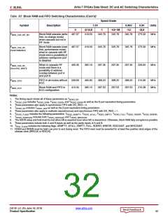
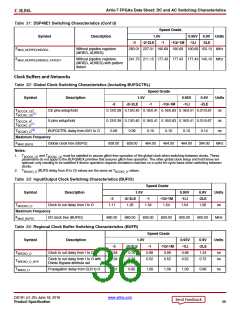
Table 31: DSP48E1 Switching Characteristics (Cont’d)
Speed Grade
1.0V
-2/-2LE
Symbol
Description
0.95V 0.9V Units
-1Q/-1M -1LI -2LE
-3
-1
FMAX_NOPIPELINEREG
Without pipeline registers
(MREG, ADREG)
260.01 227.01 190.69 190.69 190.69 150.13 MHz
FMAX_NOPIPELINEREG_PATDET
Without pipeline registers
(MREG, ADREG) with pattern
detect
241.72 211.15 177.43 177.43 177.43 140.10 MHz
Clock Buffers and Networks
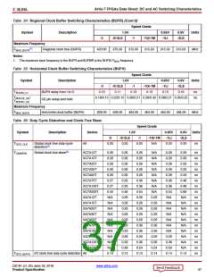
Table 32: Global Clock Switching Characteristics (Including BUFGCTRL)
Speed Grade
Symbol
Description
1.0V
-2/-2LE
0.95V
-1LI
0.9V
-2LE
Units
-3
-1
-1Q/-1M
TBCCCK_CE
/
CE pins setup/hold
0.12/0.39 0.13/0.40 0.16/0.41 0.16/0.83 0.16/0.41 0.31/0.67
ns
ns
ns
(1)
TBCCKC_CE
TBCCCK_S
/
S pins setup/hold
0.12/0.39 0.13/0.40 0.16/0.41 0.16/0.83 0.16/0.41 0.31/0.67
(1)
TBCCKC_S
(2)
TBCCKO_O
BUFGCTRL delay from I0/I1 to O
0.08
0.09
0.10
0.10
0.10
0.14
Maximum Frequency
FMAX_BUFG
Global clock tree (BUFG)
628.00
628.00
464.00
464.00
464.00
394.00
MHz
Notes:
1.
T
and T
must be satisfied to assure glitch-free operation of the global clock when switching between clocks. These
BCCCK_CE
BCCKC_CE
parameters do not apply to the BUFGMUX primitive that assures glitch-free operation. The other global clock setup and hold times are
optional; only needing to be satisfied if device operation requires simulation matches on a cycle-for-cycle basis when switching between
clocks.
2.
T
(BUFG delay from I0 to O) values are the same as T
values.
BGCKO_O
BCCKO_O
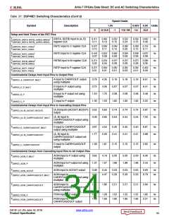
Table 33: Input/Output Clock Switching Characteristics (BUFIO)
Speed Grade
Symbol
Description
1.0V
-2/-2LE
0.95V
-1LI
0.9V
-2LE
1.56
Units
ns
-3
-1
-1Q/-1M
TBIOCKO_O
Clock to out delay from I to O
1.11
1.26
1.54
1.54
1.54
Maximum Frequency
FMAX_BUFIO I/O clock tree (BUFIO)
680.00
680.00
600.00
600.00
600.00
600.00
MHz
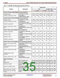
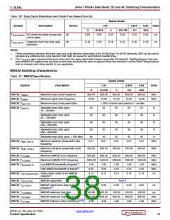
Table 34: Regional Clock Buffer Switching Characteristics (BUFR)
Speed Grade
Symbol
Description
1.0V
-2/-2LE
0.95V
-1LI
0.9V
-2LE
1.24
0.72
Units
-3
-1
-1Q/-1M
TBRCKO_O
TBRCKO_O_BYP
TBRDO_O
Clock to out delay from I to O
0.64
0.34
0.76
0.39
0.99
0.52
0.99
0.52
0.99
0.52
ns
ns
Clock to out delay from I to O with
Divide Bypass attribute set
Propagation delay from CLR to O
0.81
0.85
1.09
1.09
1.09
0.96
ns
DS181 (v1.25) June 18, 2018
www.xilinx.com
Product Specification
36

 XILINX [ XILINX, INC ]