Artix-7 FPGAs Data Sheet: DC and AC Switching Characteristics
PLL Switching Characteristics
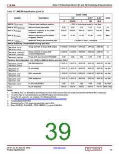
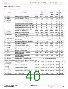
Table 38: PLL Specification
Speed Grade
Symbol
Description
1.0V
-2/-2LE
800.00
19.00
0.95V
-1LI
0.9V
-2LE
Units
-3
-1
PLL_FINMAX
PLL_FINMIN
Maximum input clock frequency
800.00
19.00
800.00
19.00
800.00
19.00
800.00
19.00
MHz
MHz
Minimum input clock frequency
PLL_FINJITTER
PLL_FINDUTY
Maximum input clock period jitter
Allowable input duty cycle: 19—49 MHz
Allowable input duty cycle: 50—199 MHz
Allowable input duty cycle: 200—399 MHz
Allowable input duty cycle: 400—499 MHz
Allowable input duty cycle: >500 MHz
Minimum PLL VCO frequency
< 20ꢀ of clock input period or 1 ns Max
25
30
25
30
25
30
25
30
25
30
ꢀ
ꢀ
35
35
35
35
35
ꢀ
40
40
40
40
40
ꢀ
45
45
45
45
45
ꢀ
PLL_FVCOMIN
800.00
800.00
800.00
800.00
800.00
MHz
MHz
MHz
MHz
ns
PLL_FVCOMAX
PLL_FBANDWIDTH
Maximum PLL VCO frequency
2133.00 1866.00 1600.00 1600.00 1600.00
Low PLL bandwidth at typical(1)
1.00
4.00
0.12
1.00
4.00
0.12
1.00
4.00
0.12
1.00
4.00
0.12
1.00
4.00
0.12
High PLL bandwidth at typical(1)
PLL_TSTATPHAOFFSET Static phase offset of the PLL outputs(2)
PLL_TOUTJITTER
PLL_TOUTDUTY
PLL_TLOCKMAX
PLL_FOUTMAX
PLL_FOUTMIN
PLL output jitter
Note 3
PLL output clock duty-cycle precision(4)
PLL maximum lock time
0.20
100.00
800.00
6.25
0.20
100.00
800.00
6.25
0.20
0.20
100.00
800.00
6.25
0.25
100.00
800.00
6.25
ns
µs
100.00
800.00
6.25
PLL maximum output frequency
PLL minimum output frequency(5)
External clock feedback variation
Minimum reset pulse width
MHz
MHz
PLL_TEXTFDVAR
PLL_RSTMINPULSE
PLL_FPFDMAX
< 20ꢀ of clock input period or 1 ns Max
5.00
5.00
5.00
5.00
5.00
ns
Maximum frequency at the phase
frequency detector
550.00
500.00
450.00
450.00
450.00
MHz
PLL_FPFDMIN
PLL_TFBDELAY
Minimum frequency at the phase
frequency detector
19.00
19.00
19.00
19.00
19.00
MHz
Maximum delay in the feedback path
3 ns Max or one CLKIN cycle
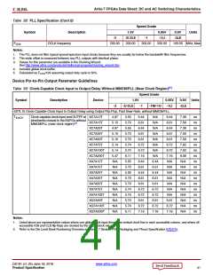
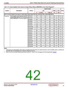
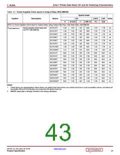
Dynamic Reconfiguration Port (DRP) for PLL Before and After DCLK
TPLLDCK_DADDR
/
Setup and hold of D address
Setup and hold of D input
Setup and hold of D enable
Setup and hold of D write enable
CLK to out of DRDY
1.25/0.15 1.40/0.15 1.63/0.15 1.63/0.15 1.43/0.00 ns, Min
1.25/0.15 1.40/0.15 1.63/0.15 1.63/0.15 1.43/0.00 ns, Min
1.76/0.00 1.97/0.00 2.29/0.00 2.29/0.00 2.40/0.00 ns, Min
1.25/0.15 1.40/0.15 1.63/0.15 1.63/0.15 1.43/0.00 ns, Min
TPLLCKD_DADDR
TPLLDCK_DI
/
TPLLCKD_DI
TPLLDCK_DEN
/
TPLLCKD_DEN
TPLLDCK_DWE
TPLLCKD_DWE
/
TPLLCKO_DRDY
0.65
0.72
0.99
0.99
0.99
ns, Max
DS181 (v1.25) June 18, 2018
www.xilinx.com
Product Specification
40

 XILINX [ XILINX, INC ]