Artix-7 FPGAs Data Sheet: DC and AC Switching Characteristics
DSP48E1 Switching Characteristics
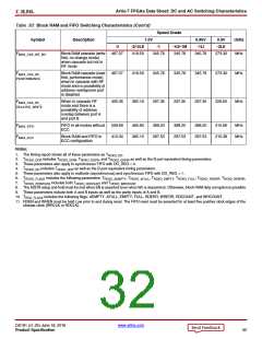
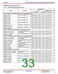
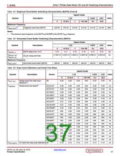
Table 31: DSP48E1 Switching Characteristics
Speed Grade
1.0V
-2/-2LE
Symbol
Description
0.95V 0.9V Units
-3
Setup and Hold Times of Data/Control Pins to the Input Register Clock
-1
-1Q/-1M -1LI
-2LE
TDSPDCK_A_AREG
/
A input to A register CLK
B input to B register CLK
C input to C register CLK
D input to D register CLK
ACIN input to A register CLK
BCIN input to B register CLK
0.26/
0.12
0.30/
0.13
0.37/
0.14
0.37/
0.28
0.37/
0.14
0.45/
0.14
ns
ns
ns
ns
ns
ns
TDSPCKD_A_AREG
TDSPDCK_B_BREG
TDSPCKD_B_BREG
/
0.33/
0.15
0.38/
0.16
0.45/
0.18
0.45/
0.25
0.45/
0.18
0.60/
0.19
TDSPDCK_C_CREG
TDSPCKD_C_CREG
/
/
0.17/
0.17
0.20/
0.19
0.24/
0.21
0.24/
0.26
0.24/
0.21
0.34/
0.29
TDSPDCK_D_DREG
TDSPCKD_D_DREG
0.25/
0.25
0.32/
0.27
0.42/
0.27
0.42/
0.42
0.42/
0.27
0.54/
0.23
TDSPDCK_ACIN_AREG
TDSPCKD_ACIN_AREG
/
/
0.23/
0.12
0.27/
0.13
0.32/
0.14
0.32/
0.17
0.32/
0.14
0.36/
0.14
TDSPDCK_BCIN_BREG
TDSPCKD_BCIN_BREG
0.25/
0.15
0.29/
0.16
0.36/
0.18
0.36/
0.18
0.36/
0.18
0.41/
0.19
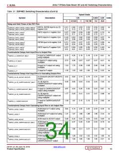
Setup and Hold Times of Data Pins to the Pipeline Register Clock
TDSPDCK_ A, B _MREG_MULT
/
{A, B} input to M register CLK
using multiplier
2.40/
–0.01
2.76/
–0.01
3.29/
–0.01
3.29/
–0.01
3.29/
–0.01 –0.07
4.31/
ns
ns
{
}
TDSPCKD_{A, B}_MREG_MULT
TDSPDCK_ A, D _ADREG
/
{A, D} input to AD register CLK
1.29/
–0.02
1.48/
–0.02
1.76/
–0.02
1.76/
–0.02
1.76/ 2.29/
–0.02 –0.27
{
}
TDSPCKD_{A, D}_ADREG
Setup and Hold Times of Data/Control Pins to the Output Register Clock
TDSPDCK_{A, B}_PREG_MULT
/
{A, B} input to P register CLK
using multiplier
4.02/
–0.28
4.60/
–0.28
5.48/
–0.28
5.48/
–0.28
5.48/
–0.28 –0.48
6.95/
ns
ns
ns
ns
ns
TDSPCKD_{A, B} _PREG_MULT
TDSPDCK_D_PREG_MULT
TDSPCKD_D_PREG_MULT
/
D input to P register CLK using
multiplier
3.93/
–0.73
4.50/
–0.73
5.35/
–0.73
5.35/
–0.73
5.35/ 6.73/
–0.73 –1.68
TDSPDCK_{A, B} _PREG
/
A or B input to P register CLK
not using multiplier
1.73/
–0.28
1.98/
–0.28
2.35/
–0.28
2.35/
–0.28
2.35/ 2.80/
TDSPCKD_{A, B} _PREG
–0.28 –0.48
2.10/ 2.54/
TDSPDCK_C_PREG
TDSPCKD_C_PREG
/
C input to P register CLK not
using multiplier
1.54/
–0.26
1.76/
–0.26
2.10/
–0.26
2.10/
–0.26
–0.26 –0.45
TDSPDCK_PCIN_PREG
/
PCIN input to P register CLK
1.32/
–0.15
1.51/
–0.15
1.80/
–0.15
1.80/
–0.15
1.80/ 2.13/
–0.15 –0.25
TDSPCKD_PCIN_PREG
Setup and Hold Times of the CE Pins
TDSPDCK_{CEA;CEB}_{AREG;BREG}
/
{CEA; CEB} input to {A; B}
register CLK
0.35/
0.06
0.42/
0.08
0.52/
0.11
0.52/
0.11
0.52/
0.11
0.64/
0.11
ns
ns
ns
ns
ns
TDSPCKD_{CEA;CEB}_{AREG;BREG}
TDSPDCK_CEC_CREG
/
/
CEC input to C register CLK
CED input to D register CLK
CEM input to M register CLK
CEP input to P register CLK
0.28/
0.10
0.34/
0.11
0.42/
0.13
0.42/
0.13
0.42/
0.13
0.49/
0.16
TDSPCKD_CEC_CREG
TDSPDCK_CED_DREG
TDSPCKD_CED_DREG
0.36/
–0.03
0.43/
–0.03
0.52/
–0.03
0.52/
–0.03
0.52/
–0.03
0.68/
0.14
TDSPDCK_CEM_MREG
TDSPCKD_CEM_MREG
/
0.17/
0.18
0.21/
0.20
0.27/
0.23
0.27/
0.23
0.27/
0.23
0.45/
0.29
TDSPDCK_CEP_PREG
/
0.36/
0.01
0.43/
0.01
0.53/
0.01
0.53/
0.01
0.53/
0.01
0.63/
0.00
TDSPCKD_CEP_PREG
DS181 (v1.25) June 18, 2018
www.xilinx.com
Product Specification
33

 XILINX [ XILINX, INC ]