Artix-7 FPGAs Data Sheet: DC and AC Switching Characteristics
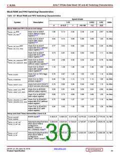
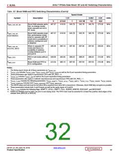
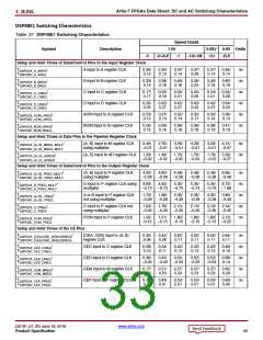
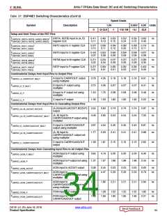
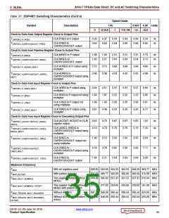
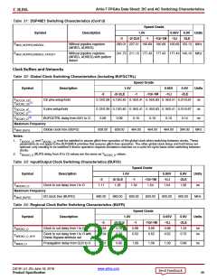
Table 30: Block RAM and FIFO Switching Characteristics (Cont’d)
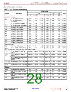
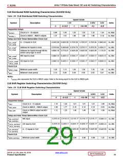
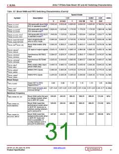
Speed Grade
Symbol
Description
1.0V
0.95V
-1LI
0.9V
-2LE
Units
-3
-2/-2LE
-1
-1Q/-1M
FMAX_CAS_WF_NC
Block RAM cascade (write
first, no change mode)
when cascade but not in
RF mode
467.07
418.59
345.78
345.78
345.78
273.30
MHz
FMAX_CAS_RF_
PERFORMANCE
Block RAM cascade (read
first, performance mode)
when in cascade with RF
mode and no possibility of
address overlap/one port
is disabled
467.07
405.35
418.59
362.19
345.78
297.35
345.78
345.78
297.35
273.30
226.60
MHz
MHz
FMAX_CAS_RF_
DELAYED_WRITE
When in cascade RF
mode and there is a
possibility of address
overlap between port A
and port B
297.35
FMAX_FIFO
FMAX_ECC
FIFO in all modes without
ECC
509.68
410.34
460.83
365.10
388.20
297.53
388.20
297.53
388.20
297.53
315.66
215.38
MHz
MHz
Block RAM and FIFO in
ECC configuration
Notes:
1. The timing report shows all of these parameters as T
.
RCKO_DO
2.
3. These parameters also apply to synchronous FIFO with DO_REG = 0.
4. includes T as well as the B port equivalent timing parameters.
5. These parameters also apply to multirate (asynchronous) and synchronous FIFO with DO_REG = 1.
T
includes T
, T
, and T
as well as the B port equivalent timing parameters.
RCKO_DOR
RCKO_DOW RCKO_DOPR
RCKO_DOPW
T
RCKO_DO
RCKO_DOP
6.
7.
T
T
includes the following parameters: T
, T , T , T , T , T
RCKO_FLAGS
RCKO_AEMPTY RCKO_AFULL RCKO_EMPTY RCKO_FULL RCKO_RDERR RCKO_WRERR.
includes both T
and T
RCKO_POINTERS
RCKO_RDCOUNT
RCKO_WRCOUNT.
8. The ADDR setup and hold must be met when EN is asserted (even when WE is deasserted). Otherwise, block RAM data corruption is possible.
9. These parameters include both A and B inputs as well as the parity inputs of A and B.
10. T
includes the following flags: AEMPTY, AFULL, EMPTY, FULL, RDERR, WRERR, RDCOUNT, and WRCOUNT.
RCO_FLAGS
11. RDEN and WREN must be held Low prior to and during reset. The FIFO reset must be asserted for at least five positive clock edges of the
slowest clock (WRCLK or RDCLK).
DS181 (v1.25) June 18, 2018
www.xilinx.com
Product Specification
32

 XILINX [ XILINX, INC ]