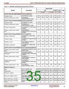
Artix-7 FPGAs Data Sheet: DC and AC Switching Characteristics
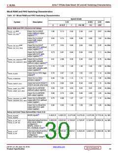
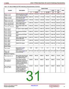
Table 30: Block RAM and FIFO Switching Characteristics (Cont’d)
Speed Grade
Symbol
Description
1.0V
0.95V
-1LI
0.9V
-2LE
Units
-3
-2/-2LE
-1
-1Q/-1M
TRDCK_DI_ECC
TRCKD_DI_ECC
/
DIN inputs with block RAM 0.50/0.43 0.55/0.46 0.63/0.50 0.63/0.50 0.63/0.50 0.78/0.54 ns, Min
ECC in standard mode(9)
TRDCK_DI_ECCW
/
DIN inputs with block RAM 0.93/0.43 1.02/0.46 1.17/0.50 1.17/0.50 1.17/0.50 1.38/0.48 ns, Min
ECC encode only(9)
TRCKD_DI_ECCW
TRDCK_DI_ECC_FIFO
/
DIN inputs with FIFO ECC 1.04/0.56 1.15/0.59 1.32/0.64 1.32/0.64 1.32/0.64 1.55/0.77 ns, Min
in standard mode(9)
TRCKD_DI_ECC_FIFO
TRCCK_INJECTBITERR
TRCKC_INJECTBITERR
/
Inject single/double bit
error in ECC mode
0.58/0.35 0.64/0.37 0.74/0.40 0.74/0.52 0.74/0.40 0.92/0.48 ns, Min
TRCCK_EN/TRCKC_EN
Block RAM enable (EN)
input
0.35/0.20 0.39/0.21 0.45/0.23 0.45/0.41 0.45/0.23 0.57/0.26 ns, Min
TRCCK_REGCE
/
CE input of output register 0.24/0.15 0.29/0.15 0.36/0.16 0.36/0.39 0.36/0.16 0.40/0.19 ns, Min
TRCKC_REGCE
TRCCK_RSTREG
TRCKC_RSTREG
/
Synchronous RSTREG
input
0.29/0.07 0.32/0.07 0.35/0.07 0.35/0.17 0.35/0.07 0.41/0.07 ns, Min
0.32/0.42 0.34/0.43 0.36/0.46 0.36/0.57 0.36/0.46 0.40/0.47 ns, Min
0.44/0.18 0.48/0.19 0.54/0.20 0.54/0.42 0.54/0.20 0.64/0.23 ns, Min
0.46/0.30 0.46/0.35 0.47/0.43 0.47/0.43 0.47/0.43 0.77/0.44 ns, Min
0.42/0.30 0.43/0.35 0.43/0.43 0.43/0.62 0.43/0.43 0.71/0.50 ns, Min
TRCCK_RSTRAM
TRCKC_RSTRAM
/
Synchronous RSTRAM
input
TRCCK_WEA
/
Write enable (WE) input
(block RAM only)
TRCKC_WEA
TRCCK_WREN
/
WREN FIFO inputs
TRCKC_WREN
TRCCK_RDEN
TRCKC_RDEN
/
RDEN FIFO inputs
Reset Delays
TRCO_FLAGS
Reset RST to FIFO
flags/pointers(10)
0.90
0.98
1.10
1.10
1.10
1.25
ns, Max
TRREC_RST
/
FIFO reset recovery and 1.87/–0.81 2.07/–0.81 2.37/–0.81 2.37/–0.58 2.37/–0.81 2.44/–0.71 ns, Max
removal timing(11)
TRREM_RST
Maximum Frequency
FMAX_BRAM_WF_NC
Block RAM (write first and
no change modes) when
not in SDP RF mode
509.68
509.68
460.83
460.83
388.20
388.20
388.20
388.20
388.20
388.20
315.66
315.66
MHz
MHz
FMAX_BRAM_RF_
PERFORMANCE
Block RAM (read first,
performance mode) when
in SDP RF mode but no
address overlap between
port A and port B
FMAX_BRAM_RF_
DELAYED_WRITE
Block RAM (read first,
delayed write mode) when
in SDP RF mode and
there is possibility of
447.63
404.53
339.67
339.67
339.67
268.96
MHz
overlap between port A
and port B addresses
DS181 (v1.25) June 18, 2018
www.xilinx.com
Product Specification
31

 XILINX [ XILINX, INC ]