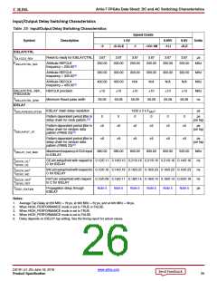
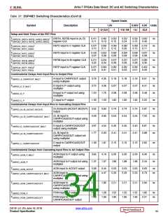
Artix-7 FPGAs Data Sheet: DC and AC Switching Characteristics
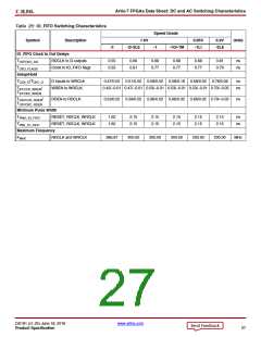
Block RAM and FIFO Switching Characteristics
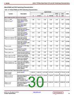
Table 30: Block RAM and FIFO Switching Characteristics
Speed Grade
Symbol
Description
1.0V
0.95V
-1LI
0.9V
-2LE
Units
-3
-2/-2LE
-1
-1Q/-1M
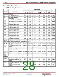
Block RAM and FIFO Clock-to-Out Delays
TRCKO_DO and
TRCKO_DO_REG
Clock CLK to DOUT
output (without output
register)(2)(3)
1.85
2.13
2.46
2.46
0.89
3.84
0.94
3.30
1.46
2.46
0.89
3.84
0.94
3.30
1.46
2.87
1.02
5.30
1.11
3.76
1.56
ns, Max
ns, Max
ns, Max
ns, Max
ns, Max
ns, Max
(1)
Clock CLK to DOUT
output (with output
register)(4)(5)
0.64
2.77
0.73
2.61
1.16
0.74
3.04
0.81
2.88
1.28
0.89
3.84
0.94
3.30
1.46
TRCKO_DO_ECC and
TRCKO_DO_ECC_REG
Clock CLK to DOUT
output with ECC (without
output register)(2)(3)
Clock CLK to DOUT
output with ECC (with
output register)(4)(5)
TRCKO_DO_CASCOUT and Clock CLK to DOUT
output with cascade
TRCKO_DO_CASCOUT_REG
(without output register)(2)
Clock CLK to DOUT
output with cascade (with
output register)(4)
TRCKO_FLAGS
Clock CLK to FIFO flags
outputs(6)
0.76
0.94
0.78
2.56
0.68
0.75
0.87
1.02
0.85
2.81
0.76
0.88
1.05
1.15
0.94
3.55
0.89
1.07
1.05
1.15
0.94
3.55
0.89
1.07
1.05
1.15
0.94
3.55
0.89
1.07
1.14
1.30
1.10
4.90
1.05
1.15
ns, Max
ns, Max
ns, Max
ns, Max
ns, Max
ns, Max
TRCKO_POINTERS
TRCKO_PARITY_ECC
Clock CLK to FIFO
pointers outputs(7)
ClockCLKtoECCPARITY
in ECC encode only mode
TRCKO_SDBIT_ECC and
TRCKO_SDBIT_ECC_REG
Clock CLK to BITERR
(without output register)
Clock CLK to BITERR
(with output register)
TRCKO_RDADDR_ECC and Clock CLK to RDADDR
TRCKO_RDADDR_ECC_REG output with ECC (without
output register)
Clock CLK to RDADDR
output with ECC (with
output register)
0.84
0.93
1.08
1.08
1.08
1.29
ns, Max
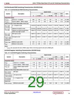
Setup and Hold Times Before/After Clock CLK
TRCCK_ADDRA
/
ADDR inputs(8)
0.45/0.31 0.49/0.33 0.57/0.36 0.57/0.52 0.57/0.36 0.77/0.45 ns, Min
TRCKC_ADDRA
TRDCK_DI_WF_NC
TRCKD_DI_WF_NC
/
Data input setup/hold time 0.58/0.60 0.65/0.63 0.74/0.67 0.74/0.67 0.74/0.67 0.92/0.76 ns, Min
when block RAM is
configured in
WRITE_FIRST or
NO_CHANGE mode(9)
TRDCK_DI_RF
/
Data input setup/hold time 0.20/0.29 0.22/0.34 0.25/0.41 0.25/0.50 0.25/0.41 0.29/0.38 ns, Min
TRCKD_DI_RF
when block RAM is
configured in
READ_FIRST mode(9)
DS181 (v1.25) June 18, 2018
www.xilinx.com
Product Specification
30

 XILINX [ XILINX, INC ]