Spartan-3E FPGA Family: DC and Switching Characteristics
Serial Peripheral Interface (SPI) Configuration Timing
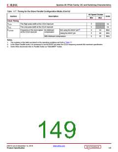
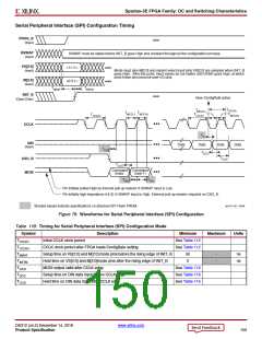
X-Ref Target - Figure 76
PROG_B
(Input)
HSWAP
(Input)
HSWAP must be stable before INIT_B goes High and constant throughout the configuration process.
VS[2:0]
(Input)
<1:1:1>
Mode input pins M[2:0] and variant select input pins VS[2:0] are sampled when INIT_B
goes High. After this point, input values do not matter until DONE goes High, at which
point these pins become user-I/O pins.
M[2:0]
(Input)
<0:0:1>
TMINIT
TINITM
INIT_B
(Open-Drain)
New ConfigRate active
TCCLK
TMCCH
T
n
MCCL
n
TMCCL1 TMCCH1
T
TCCLK1
CCLK1
n
CCLK
TV
DIN
(Input)
Data
Data
TDCC
Data
Data
TCSS
TCCD
CSO_B
MOSI
TCCO
Command Command
(msb) (msb-1)
TDSU
TDH
Pin initially pulled High by internal pull-up resistor if HSWAP input is Low.
Pin initially high-impedance (Hi-Z) if HSWAP input is High. External pull-up resistor required on CSO_B.
ds312-3_06_110206
Shaded values indicate specifications on attached SPI Flash PROM.
Figure 76: Waveforms for Serial Peripheral Interface (SPI) Configuration
Table 118: Timing for Serial Peripheral Interface (SPI) Configuration Mode
Symbol Description
TCCLK1
Minimum
See Table 112
See Table 112
50
Maximum
Units
Initial CCLK clock period
TCCLKn
TMINIT
TINITM
TCCO
CCLK clock period after FPGA loads ConfigRate setting
Setup time on VS[2:0] and M[2:0] mode pins before the rising edge of INIT_B
Hold time on VS[2:0] and M[2:0]mode pins after the rising edge of INIT_B
MOSI output valid after CCLK edge
-
-
ns
ns
0
See Table 116
See Table 116
See Table 116
TDCC
Setup time on DIN data input before CCLK edge
TCCD
Hold time on DIN data input after CCLK edge
DS312 (v4.2) December 14, 2018
www.xilinx.com
Product Specification
150

 XILINX [ XILINX, INC ]