Spartan-3E FPGA Family: DC and Switching Characteristics
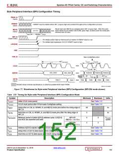
Byte Peripheral Interface (BPI) Configuration Timing
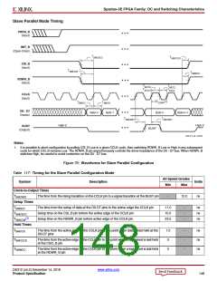
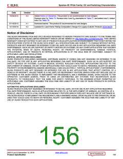
X-Ref Target - Figure 77
PROG_B
(Input)
HSWAP
HSWAP must be stable before INIT_B goes High and constant throughout the configuration process.
Mode input pins M[2:0] are sampled when INIT_B goes High. After this point,
(Input)
M[2:0]
(Input)
<0:1:0>
input values do not matter until DONE goes High, at which point the mode pins
become user-I/O pins.
TMINIT
TINITM
INIT_B
(Open-Drain)
Pin initially pulled High by internal pull-up resistor if HSWAP input is Low.
Pin initially high-impedance (Hi-Z) if HSWAP input is High.
LDC[2:0]
HDC
CSO_B
New ConfigRate active
TCCLK1
TCCLKn
TINITADDR
TCCLK1
CCLK
TCCO
000_0000
Address
Address Address
TCCD
A[23:0]
000_0001
T
TDCC
Data
AVQV
D[7:0]
(Input)
Byte 0
Data
Data
Data
Byte 1
Shaded values indicate specifications on attached parallel NOR Flash PROM.
DS312-3_08_032409
Figure 77: Waveforms for Byte-wide Peripheral Interface (BPI) Configuration (BPI-DN mode shown)
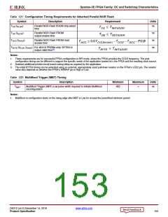
Table 120: Timing for Byte-wide Peripheral Interface (BPI) Configuration Mode
Symbol
TCCLK1
TCCLKn
TMINIT
Description
Minimum
Maximum
See Table 112
See Table 112
-
Units
Initial CCLK clock period
CCLK clock period after FPGA loads ConfigRate setting
Setup time on CSI_B, RDWR_B, and M[2:0] mode pins before the rising edge of
INIT_B
50
0
ns
ns
TINITM
Hold time on CSI_B, RDWR_B, and M[2:0] mode pins after the rising edge of
INIT_B
-
TINITADDR
Minimum period of initial A[23:0] address cycle; LDC[2:0]
and HDC are asserted and valid
BPI-UP:
(M[2:0] = <0:1:0>)
5
5
2
TCCLK1
cycles
BPI-DN:
2
(M[2:0] = <0:1:1>)
TCCO
TDCC
TCCD
Address A[23:0] outputs valid after CCLK falling edge
Setup time on D[7:0] data inputs before CCLK rising edge
Hold time on D[7:0] data inputs after CCLK rising edge
See Table 116
See Table 116
See Table 116
DS312 (v4.2) December 14, 2018
www.xilinx.com
Product Specification
152

 XILINX [ XILINX, INC ]