Spartan-3E FPGA Family: DC and Switching Characteristics
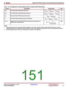
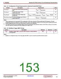
Table 121: Configuration Timing Requirements for Attached Parallel NOR Flash
Symbol
TCE (tELQV
Description
Requirement
Units
)
Parallel NOR Flash PROM chip-select
time
ns
TCE ≤ TINITADDR
TOE (tGLQV
ACC (tAVQV
TBYTE (tFLQV, FHQV
)
Parallel NOR Flash PROM
output-enable time
ns
ns
ns
TOE ≤ TINITADDR
TACC ≤ 0.5TCCLKn(min) – TCCO – TDCC – PCB
TBYTE ≤ TINITADDR
T
)
Parallel NOR Flash PROM read
access time
t
) For x8/x16 PROMs only: BYTE# to
output valid time(3)
Notes:
1. These requirements are for successful FPGA configuration in BPI mode, where the FPGA provides the CCLK frequency. The post
configuration timing can be different to support the specific needs of the application loaded int o the FPGA and the resulting clock source.
2. Subtract additional printed circuit board routing delay as required by the application.
3. The initial BYTE# timing can be extended using an external, appropriately sized pull-down resistor on the FPGA’s LDC2 pin. The resistor
value also depends on whether the FPGA’s HSWAP pin is High or Low.
Table 122: MultiBoot Trigger (MBT) Timing
Symbol
Description
Minimum
Maximum
Units
TMBT
MultiBoot Trigger (MBT) Low pulse width required to initiate MultiBoot
reconfiguration
300
∞
ns
Notes:
1. MultiBoot re-configuration starts on the rising edge after MBT is Low for at least the prescribed minimum period.
DS312 (v4.2) December 14, 2018
www.xilinx.com
Product Specification
153

 XILINX [ XILINX, INC ]